Method for smart conversion and calibration of coordinate

a coordinate and conversion technology, applied in semiconductor/solid-state device testing/measurement, image enhancement, instruments, etc., can solve the problems of product open or short failure, and large quantity of random defects and systematic defects, so as to achieve more accurate calibration of defect size value, precise killer defect index, and high accuracy

Active Publication Date: 2021-07-29
ELITETECH TECH
View PDF1 Cites 4 Cited by
  • Summary
  • Abstract
  • Description
  • Claims
  • Application Information

AI Technical Summary

Benefits of technology

The invention is a tool that uses an integrated circuit design layout and defect inspection tool to create a more accurate killer defect index. By calibrating the defect size and coordinate deviation, the tool can identify killer defects with higher accuracy and reduce incorrect judgment. This invention can serve as an important tool for identifying defects that belong to a killer or non-killer category.

Problems solved by technology

During the manufacturing stage, the random defect and systematic defect are normally created due to such factors as the equipment's precision deviation itself, abnormal failure, particle created in the process, insufficient process window in the design layout and lithography process matrix window check.
Those random defect and systematic defect will cause product's open or short failure.
Following semiconductor technology geometry shrinkage, the random defect and systematic defect will increase in large quantity with shrinkage geometry dimension.
Because the defect processing throughput is limited by the defect images throughput taken from Scanning Electron Microscope.
That makes defect sample selection of real open circuit failure defect or short circuit failure defect extremely difficult.
Normally, real open circuit failure defect or short circuit failure defect SEM images cannot be found in time to process engineer or the SEM images are useless without failure.
So, process engineer can hardly judge where the root cause of wafer yield failure is based on the SEM images.
The defect yield improvement efficiency is poor.
This will increase semiconductor fab cost.
But it becomes very hard to identify failure killer defect for the previous method in the nanometer semiconductor fab process.
Furthermore, there is defect size deviation issue between the defect contour's metrology data measured on the defect image pattern which is generated from the SEM and optical microscope and defect data generated from the defect inspection tool.
That will result in the defect size deviation issue between the defect size of the defect inspection data and the real defect size data of the SEM image.
Besides, design layout pattern geometry size keeps on shrinking in more advanced complex semiconductor process.
Especially, lithography process window is getting narrower when optical limitation effect is getting worse.
That becomes worse when the IC design layout polygon counts are increased in multiple times and layout patterns are drawn in more complex mode.
So, some defects are related to certain design layout patterns which are detected from systematic defect inspection.
Those defects that will impact yield are so-called systematic defect.
It will cause very low yield.
That blocks the opportunity to find out the real open failure or short failure defect pattern.
This defect size deviation will result in incorrect KDI value, i.e. higher KDI value than real KDI value.

Method used


Image

  • Method for smart conversion and calibration of coordinate
  • Method for smart conversion and calibration of coordinate
  • Method for smart conversion and calibration of coordinate

Examples


Embodiment Construction

[0027]In semiconductor wafer fab, semiconductor assembly fab, flat panel display fab, solar panel fab, printed circuit board fab, mask fab, LED fab or LED assembly fab, there must be run through mask, lithography, etching, and film deposition, etc. equipment and processing method to form a specific functioning product. Because there are many complex process steps in the manufacturing procedures, the process and equipment parameter control, equipment parameter shift, or technical bottleneck can produce the defects that would impact yield. Generation of those defects is inevitable. So, in the manufacturing procedures of a semiconductor fab, fab team would always execute defect inspection and analysis to improve yield and reduce cost.

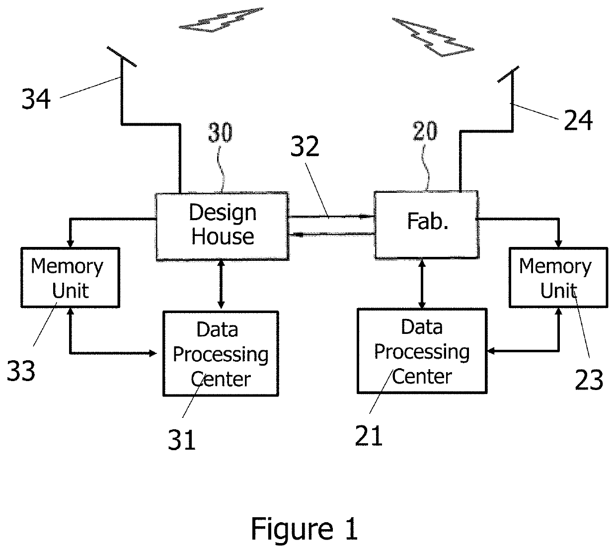
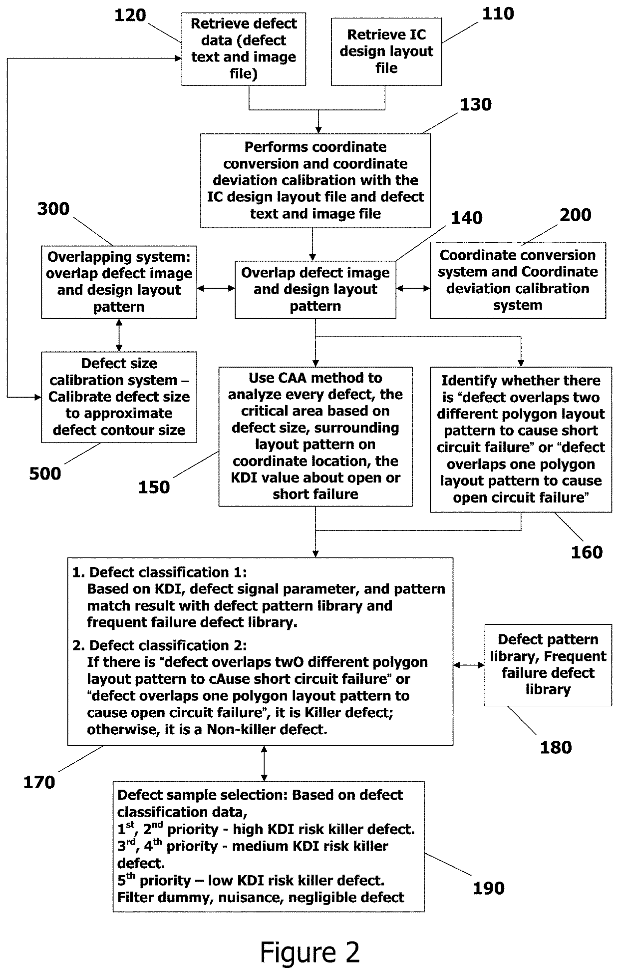
[0028]First of all, please review FIG. 1. It is an operation architecture chart for the present invention that involves a smart semiconductor defect calibration, classification, and sampling system and the method thereof. As shown in FIG. 1, a practice exa...


PUM

PropertyMeasurementUnit
defect size dimensionaaaaaaaaaa
dimensionaaaaaaaaaa
spacingaaaaaaaaaa

Abstract

The present invention relates to a smart conversion and calibration of the defect coordinate, diagnosis, sampling system and the method thereof for manufacturing fab is provided. The intelligent defect diagnosis method comprises: receiving pluralities of defect data, design layout data, analyzing the defect data, design layouts, by a Critical Area Analysis (CAA) system, wherein the analyzing step further contains the sub-steps: superposing the defect contour pattern and the design layout, performing CAA to identify a killer or non-killer defect based on the open or short failure probability, defects are classified as high, medium, low, or negligible risk defect based on the Killer Defect Index, defect signal parameters, selecting defect samples based on the defect classification data, selecting alarm defect and filtering false defect with pattern match with defect pattern library and frequent failure defect library, performing coordinate conversion and pattern match between image contour and design layout for coordinate correction, creating a CAA accuracy correction system and defect size calibration system by analyzing original defect size data and defect contour size from image analysis, evaluating the defect size using measurement uncertainty analysis with statistical analysis methods to reach the purposes of increasing CAA accuracy and Killer Defect identification rate.

Description

CROSS-REFERENCE TO RELATED APPLICATIONS[0001]This application is a continuation application of U.S. patent application Ser. No. 16 / 134,114 filed on Sep. 18, 2018, which claims the benefit of U.S. Patent Application No. 62 / 559,784 filed on Sep. 18, 2017, the content of which are hereby incorporated by reference in their entirety.BACKGROUND OF THE INVENTION1. Field of the Invention[0002]The present invention involves a smart semiconductor defect calibration, classification, and sampling system and the method thereof. Especially it is a smart defect calibration, classification, and sampling system and the method thereof applied to the semiconductor manufacturing fab, semiconductor assembly fab, flat panel display manufacturing fab, solar panel manufacturing fab, printed circuit board manufacturing fab, mask manufacturing fab, LED fab or assembly fab.2. Description of the Prior Art[0003]In general, the manufacturing of integrated circuit wafer in a semiconductor fab includes processing ...

Claims


Application Information

Patent Timeline
Patent Type & Authority Applications(United States)
IPC IPC(8): G01N21/95H01L21/66G06T7/00G01N21/88G06F30/398G06F30/3323
CPCG01N21/9501H01L22/12G06T7/001G01N21/8851H01L22/20G01N2021/8864G06F30/3323G06T2207/30148G01N2021/8874G01N2021/8861G06F30/398
Inventor LEU, IYUNTSAY, RAY JENN
Owner ELITETECH TECH
Why Eureka
Try Eureka