Bevel peeling and defectivity solution for substrate processing

Pending Publication Date: 2020-11-19
APPLIED MATERIALS INC
View PDF0 Cites 0 Cited by
  • Summary
  • Abstract
  • Description
  • Claims
  • Application Information

AI Technical Summary

Benefits of technology

The patent text describes methods and tools for preventing defects in semiconductor devices caused by peeling of material from the surfaces of a substrate during deposition. This reduces the production of particulate defects and improves the manufacturing process.

Problems solved by technology

Integrated circuits have evolved into complex devices that can include millions of transistors, capacitors, and resistors on a single chip.
Such thin resist layers can be insufficient to mask underlying material layers during the pattern transfer process due to attack by the chemical etchant.
Often, hardmask materials deposited onto the substrate surface are also undesirably deposited onto the upper and lower surfaces of the circumferential edge of the substrate, e.g., the circumferential bevel edge of the substrate.
When the deposited hardmask material is weakly adhered to the underlying substrate material the hardmask material may delaminate from the bevel surfaces and cause undesirable particulate defectivity to transfer to the active surface of the substrate where it can ultimately cause failure of the to-be-formed devices.

Method used


Image

  • Bevel peeling and defectivity solution for substrate processing
  • Bevel peeling and defectivity solution for substrate processing
  • Bevel peeling and defectivity solution for substrate processing

Examples


Embodiment Construction

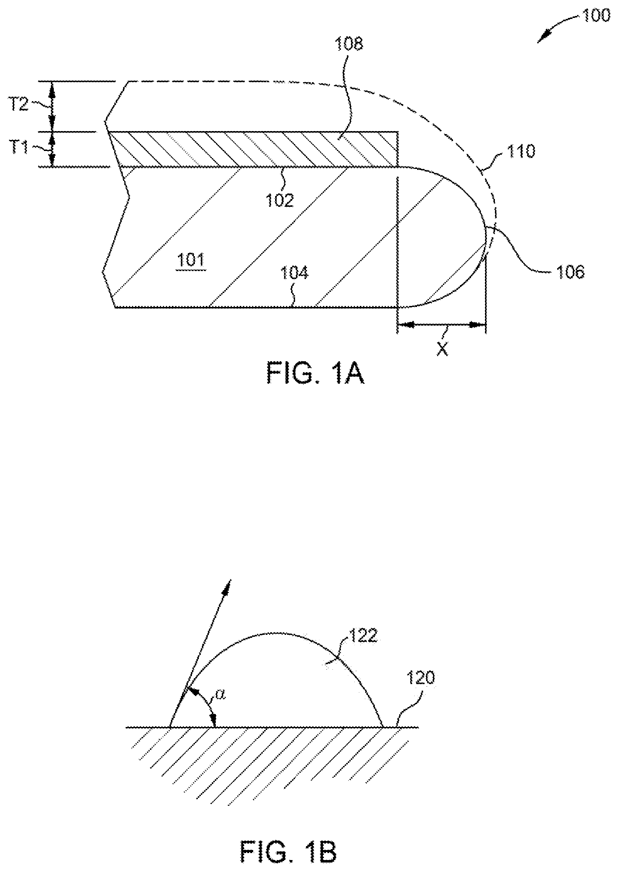
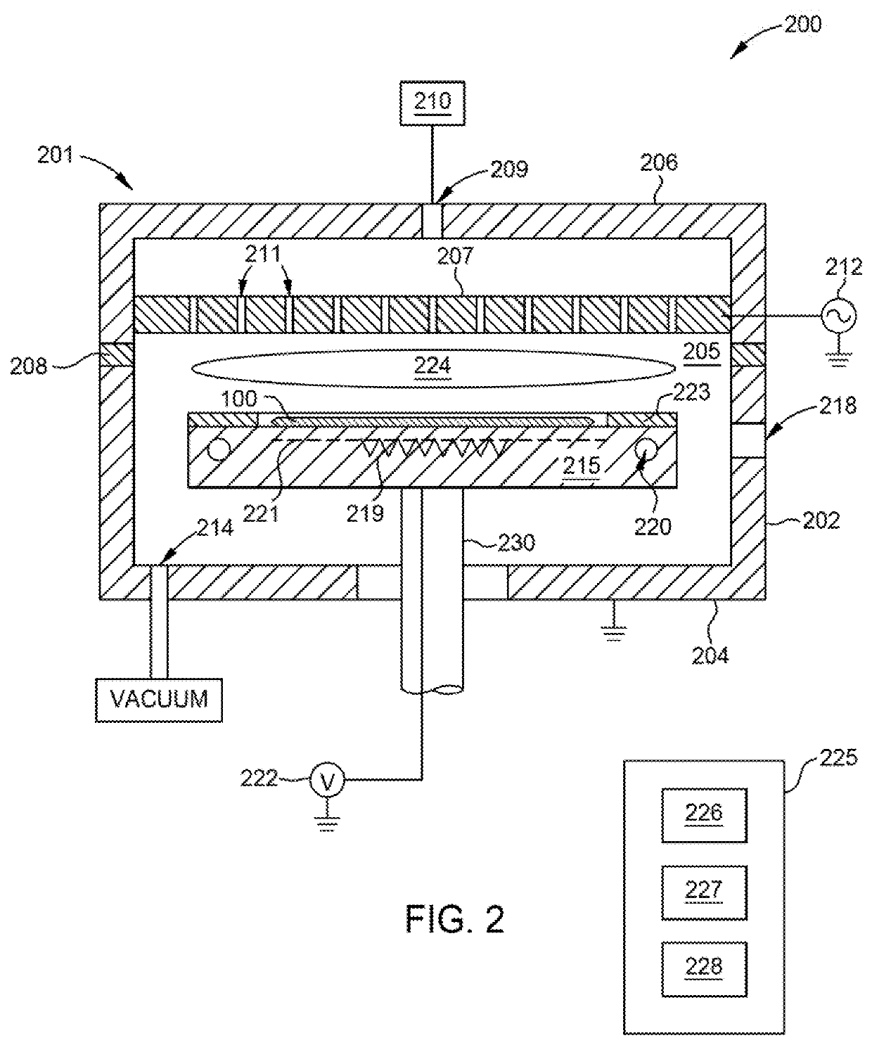
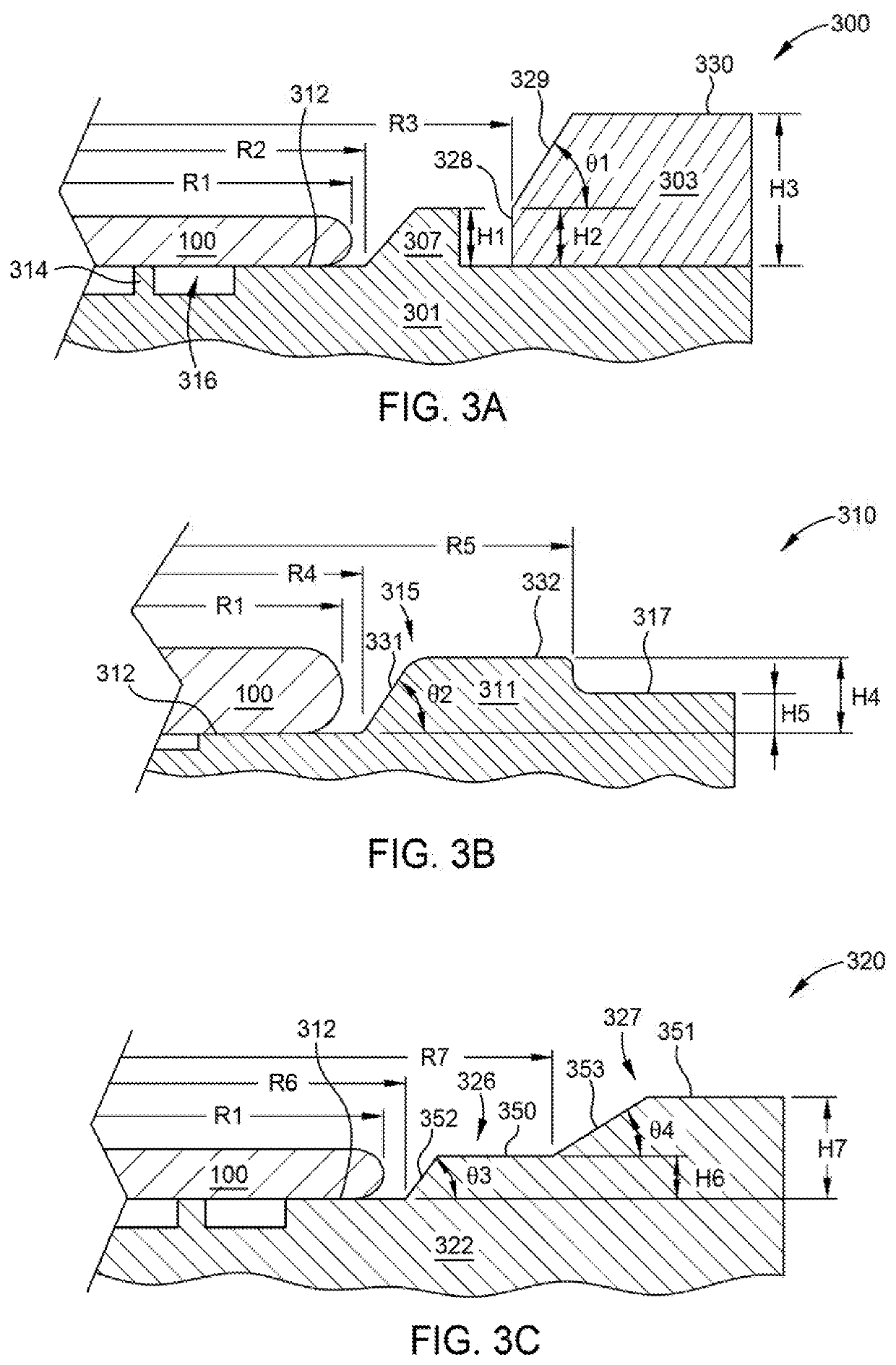
[0019]Embodiments herein relate to methods and apparatus for reducing or substantially eliminating post deposition material delamination from the bevel surfaces of a substrate (bevel peeling) thus reducing or substantially eliminating particulate defectivity associated therewith. Generally, the methods include pre-treating the substrate surface and more particularly, a bevel edge of the substrate surface, prior to a material deposition process to improve adhesion between the subsequently deposited material layer and the bevel edge surfaces. In some embodiments, the methods incorporate hardware configurations, e.g., substrate support assemblies, which prevent or substantially reduce undesired material deposition on the circumferential edge of substrate. In some embodiments, the methods and hardware configurations are used, alone or in combination, to reduce and / or substantially eliminate delamination of carbon hard mask material from the bevel edge of a substrate. For example, in som...


PUM

PropertyMeasurementUnit
Temperatureaaaaaaaaaa
Timeaaaaaaaaaa
Angleaaaaaaaaaa

Abstract

A method and apparatus for reducing bevel peeling during and after plasma enhanced chemical vapor deposition (PECVD) of a material layer on a substrate is disclosed. In one embodiment a method of processing a substrate includes positioning a substrate in a processing volume of a processing chamber, plasma treating the surface of the substrate with a treatment plasma formed of a treatment gas, chucking the substrate to the substrate support, and depositing a material layer onto the surface of the substrate by exposing the surface of the substrate to a deposition plasma. Here, the treatment gas is substantially free of carbon, silicon, or metal deposition precursors, and an RF power used to form the treatment plasma is less than about 1.42 Watts per cm2 of substrate surface (W / cm2). The deposition plasma is formed from one or a combination of a carbon, silicon, or metal precursors, and an RF power used to ignite and maintain the deposition plasma is more than about 2.12 W / cm2.

Description

CROSS-REFERENCE TO RELATED APPLICATIONS[0001]This application claims priority to U.S. Provisional Patent Application Ser. No. 62 / 848,436 filed on May 15, 2019, which is herein incorporated by reference in its entirety.BACKGROUNDField[0002]Embodiments described herein generally relate to the field of semiconductor device fabrication.Description of the Related Art[0003]Integrated circuits have evolved into complex devices that can include millions of transistors, capacitors, and resistors on a single chip. The evolution of chip designs continually involve faster circuitry and greater circuit density. The demands for faster circuits with greater circuit densities impose corresponding demands on the materials used to fabricate such integrated circuits. In particular, as the dimensions of integrated circuit components are reduced to the sub-micron scale, low resistivity conductive materials, as well as low dielectric constant insulating materials are used to obtain suitable electrical pe...

Claims


Application Information

Patent Timeline
IPC IPC(8): H01L21/02H01J37/32C23C16/04
CPCH01J2237/3328C23C16/042H01L21/0262H01J2237/3321H01J37/32642H01L21/02658H01J37/32174H01L21/31144H01L21/02315H01L21/02274H01L21/02115C23C16/0245C23C16/5096C23C16/26C23C16/4585C23C16/0209
Inventor KHAJA, ABDUL AZIZ
Owner APPLIED MATERIALS INC
Why Eureka
Try Eureka