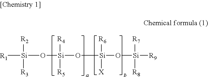
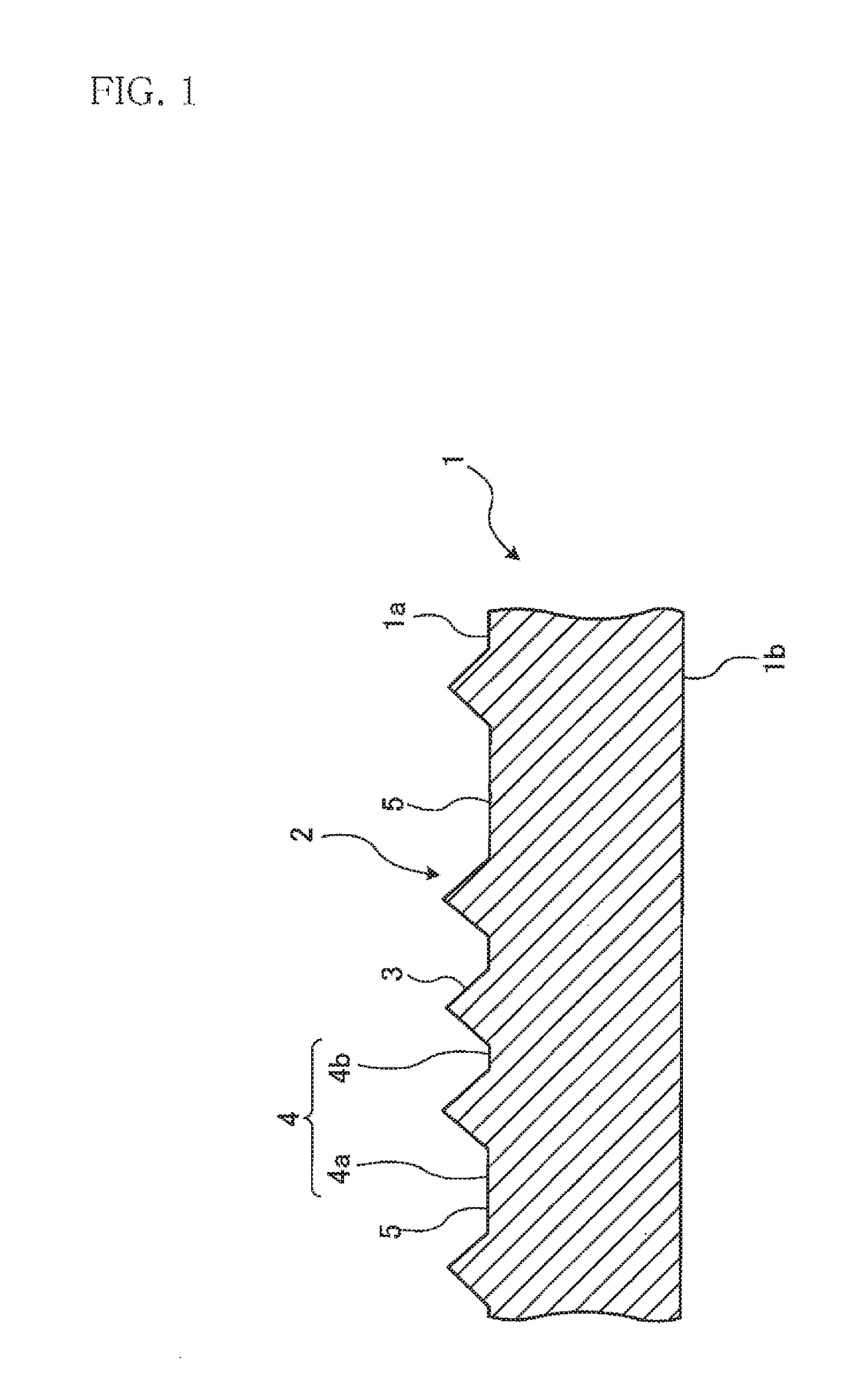
Optical substrate, substrate for semiconductor light emitting device and semiconductor light emitting device
a technology of optical substrate and semiconductor light, which is applied in the direction of semiconductor/solid-state device manufacturing, semiconductor devices, electrical devices, etc., can solve the problems of crystal dislocation defects occur by lattice mismatch, internal quantum efficiency decrease, etc., to improve internal quantum efficiency iqe, improve crystal quality, and reduce crystal dislocation defects
- Summary
- Abstract
- Description
- Claims
- Application Information
AI Technical Summary
Benefits of technology
Problems solved by technology
Method used
Image
Examples
examples
[0348]The present invention will be described below more specifically based on Examples performed to clarify the effects of the present invention. In addition, the present invention is not limited by the following Examples at all.
examples 1 to 3
[0349]First, a substrate (optical substrate) for LED was prepared. A pattern of the substrate for LED was prepared using a nano-processing sheet. The nano-processing sheet will be described later. A c-plane sapphire of 2 inches with a mirror plane on one side was prepared and cleaned. Then, the sapphire was disposed on a hot plate at 120° C. Next, the nano-processing sheet was bonded to the sapphire, using a laminate roll heated to 120° C. Bonding was performed at a pressure of 0.5 MPa and at a linear velocity of 50 mm / sec. The sapphire with the nano-processing sheet bonded was irradiated with ultraviolet light over the sapphire. The ultraviolet light was applied from a UV-LED light source with a wavelength of 365 nm, and was set so that the integral light amount was 1500 mJ / cm2. Next, the nano-processing sheet and sapphire were nipped between two parallel plates heated to 120° C. The pressure in the nip was 0.3 MPa, and the time was 10 seconds. Then, the resultant was cooled to roo...
example 5
[0390]The sapphire substrate prepared in Example 4 was placed inside a MOCVD apparatus to prepare LEDs. First, the substrate was heated in an atmosphere of hydrogen, and the surface was cleaned. Then, the low-temperature growth buffer layer of AlxGa1-xN (0≤x≤1) was deposited in 200 Å. Next, an undoped GaN layer was deposited, the raw material composition ratio, deposition temperature and deposition pressure were adjusted as appropriate, and while filling the concavities and convexities on the surface of the sapphire substrate with the GaN layer, a flattened undoped GaN layer was obtained.
[0391]The crystal quality of the undoped GaN layer was evaluated, by measuring the X-ray rocking curve full width at half maximum (XRC-FWHM) of GaN (102).
(XRC)
[0392]Apparatus: X-Ray diffractometer SmartLab[0393](made by Rigaku)
[0394]Tube voltage: 45 keV
[0395]Tube current: 200 mA
[0396]Next, as an n-type GaN layer, Si-doped GaN was deposited. Next, a strain compensation layer was provided. Subsequentl...
PUM
 Abstract
Description
Claims
Application Information
 - R&D
- Intellectual Property
- Life Sciences
- Materials
- Tech Scout
- Unparalleled Data Quality
- Higher Quality Content
- 60% Fewer Hallucinations
Browse by: Latest US Patents, China's latest patents, Technical Efficacy Thesaurus, Application Domain, Technology Topic, Popular Technical Reports.
© 2025 PatSnap. All rights reserved.Legal|Privacy policy|Modern Slavery Act Transparency Statement|Sitemap|About US| Contact US: help@patsnap.com


