
Apparatus, method and computer program product for defect detection in work pieces

a technology for defect detection and work pieces, applied in the field of apparatus for defect detection of work pieces, can solve the problems of significant drawbacks in the setup of fig. 1, side cracks created by the dicing process, embedded cracks created, etc., and achieve the effects of increasing signal to noise, fast inspection solutions, and high contras

Active Publication Date: 2016-10-27
KLA TENCOR TECH CORP
View PDF10 Cites 10 Cited by
  • Summary
  • Abstract
  • Description
  • Claims
  • Application Information

AI Technical Summary

Benefits of technology

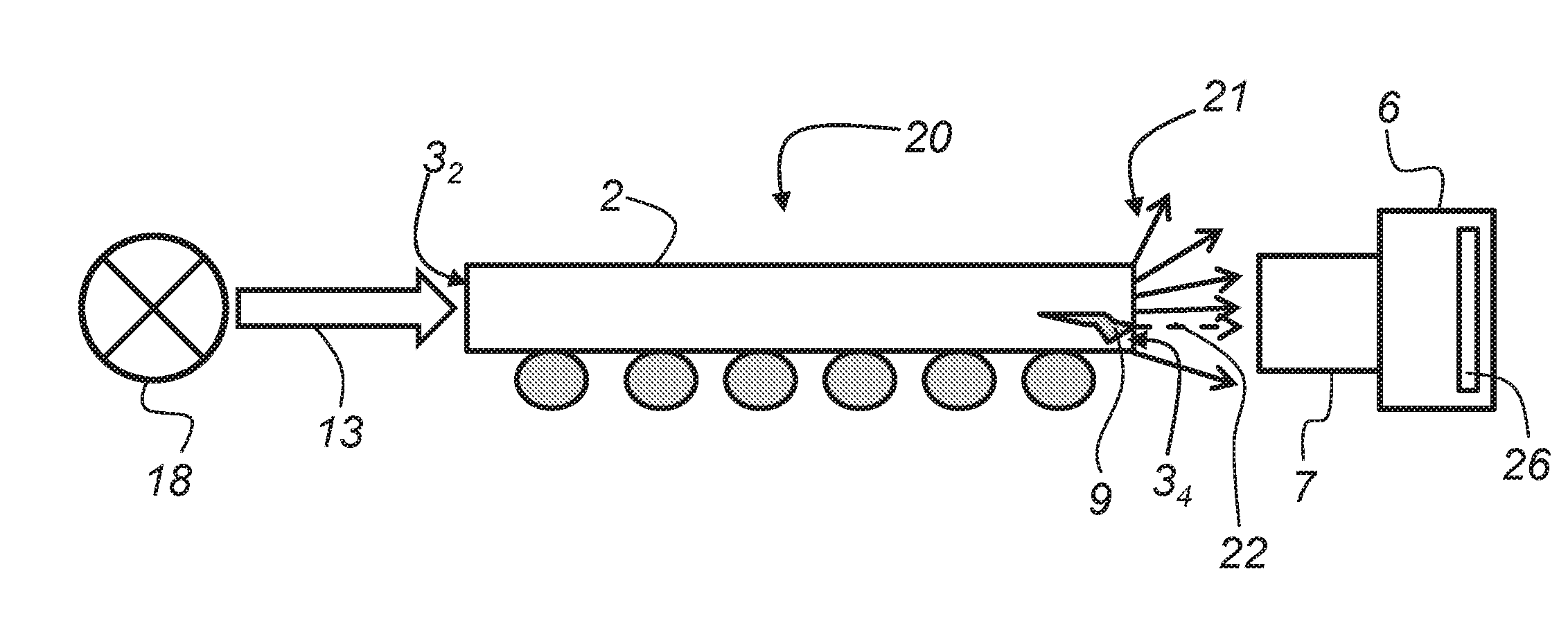
The patent describes a method for inspecting semiconductor devices using infrared light. The method allows for creating images of defects by using IR light that travels through the semiconductor device and a perpendicular or angular setup. The method utilizes the high refractive index of silicon and the rough edge of the device to create a diffuse illumination, which acts like a filter to remove noise. The method can be used with both the front and edges of the device. By looking only at the side face, the method creates opportunities for increased resolution and faster inspection. The method includes applying the illumination light on one side face of the device and using the IR light to provide an “angular side view” or an “IR back view” to inspect interior or side defects. The method reduces the response to external contamination and increases the signal to noise ratio for real defects.

Problems solved by technology

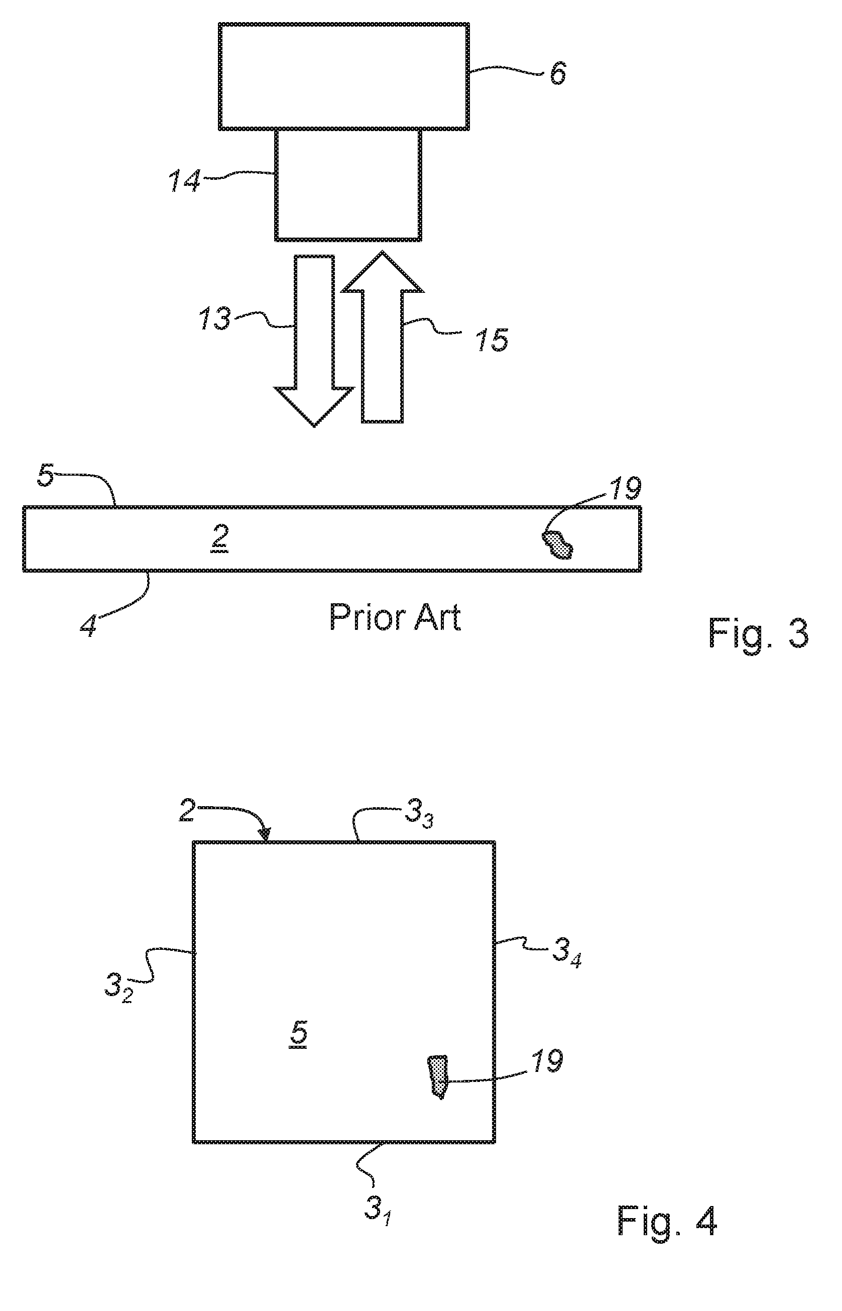
Typical defects are side cracks created by the dicing process or embedded cracks created by internal stress in the device between the dielectric layer and the silicon structure.
Additionally, the setup of FIG. 1 has significant drawbacks.
Additionally, the image resolution of the four-sided view requires a large field of view and this will limit the pixel resolution that can be used.
Therefore it is not possible to have good focus and a high resolution in order to discriminate a real defect from non-critical contamination.
First of all the method is slow.
If one wanted to automate this and make it faster there is an important limitation in the size and the number of pixels of the available IR cameras 6.
Additionally, it only works for a limited set of devices where there is a bare silicon side to apply the IR light.
A further drawback is the signal to noise ratio.
This prior art method, described above, has significant drawbacks by inspecting five sides of a work piece (singulated semiconductor device).
One drawback is the differing focus between the side face and the bottom face of the work piece.
A further drawback is the image resolution.
A view of the four side faces requires a large field of view and this will limit the pixel resolution that can be used.

Method used


Image

  • Apparatus, method and computer program product for defect detection in work pieces
  • Apparatus, method and computer program product for defect detection in work pieces
  • Apparatus, method and computer program product for defect detection in work pieces

Examples


Embodiment Construction

[0078]In the figures like reference numerals are used for like elements or elements of like function. Furthermore, for the sake of clarity, only those reference numerals are shown in the figures which are necessary for discussing the respective figure. The methods and apparatus described herein may be employed advantageously in conjunction with IR-light for defect inspection in semiconductor devices. Typically one would use IR light to be able to penetrate through the silicon of the semiconductor device. In other embodiments of the invention the wavelength of the light source could change. The only prerequisite is that the material of the work piece (semiconductor device) under inspection must be transparent for the wavelength range used. The description below refers to semiconductor devices, which should not be understood as a limitation of the invention. As is clear for a skilled person, the principles and ideas of the present invention are applicable to any inspection of internal...


PUM

PropertyMeasurementUnit
band gapaaaaaaaaaa
wavelengthsaaaaaaaaaa
anglesaaaaaaaaaa

Abstract

An apparatus, a method and a computer program product for defect detection in work pieces is disclosed. At least one light source is provided and the light source generates an illumination light of a wavelength range at which the work piece is transparent. A camera images the light from at least one face of the work piece on a detector of the camera by means of a lens. A stage is used for moving the work piece and for imaging the at least one face of the semiconductor device completely with the camera. The computer program product is disposed on a non-transitory, computer readable medium for defect detection in work pieces. A computer is used to execute the various process steps and to control the various means of the apparatus.

Description

CROSS REFERENCE TO RELATED APPLICATIONS[0001]This application is filed under 35 U.S.C. §120 and §365(c) as a continuation of International Patent Application Serial No. PCT / US2015 / 064100, filed on Dec. 4, 2015, which application claims the benefit under 35 U.S.C. §119(e) of U.S. Provisional Patent Application No. 62 / 088,284 filed on Dec. 5, 2014 and U.S. Provisional Patent Application No. 62 / 154,109 filed on Apr. 28, 2015, which applications are incorporated herein by reference in their entireties.FIELD OF THE INVENTION[0002]The present invention refers to an apparatus for defect detection in work pieces.[0003]Furthermore, the present invention refers to a method for defect detection in work pieces.[0004]Additionally, the present invention refers to a computer program product disposed on a non-transitory computer readable medium, the product comprising computer executable process steps operable to control a computer for defect detection in work pieces.BACKGROUND OF THE INVENTION[000...

Claims


Application Information

Patent Timeline
Patent Type & Authority Applications(United States)
IPC IPC(8): G01N21/95G01R31/01
CPCG01N21/9501G01N21/8806G01N21/95G01N21/9505G01N21/95684G01R31/01G01N21/8851G01N2021/8835G01N2021/8841G01N2201/1047G01R31/26G01R31/28
Inventor MARIVOET, TOMTRUYENS, CARLWOUTERS, CHRISTOPHE
Owner KLA TENCOR TECH CORP
Learn More