Field-effect transistor, method for manufacturing same, and sputtering target
a field effect transistor and sputtering target technology, applied in the direction of electrolysis components, vacuum evaporation coatings, coatings, etc., can solve the problems of difficult application of the same to a large-area substrate, large amount of energy and a large number of steps, and large amount of production steps. , to achieve the effect of reducing the number of masks, reducing production costs, and reducing production costs
- Summary
- Abstract
- Description
- Claims
- Application Information
AI Technical Summary
Benefits of technology
Problems solved by technology
Method used
Image
Examples
examples 1 to 17
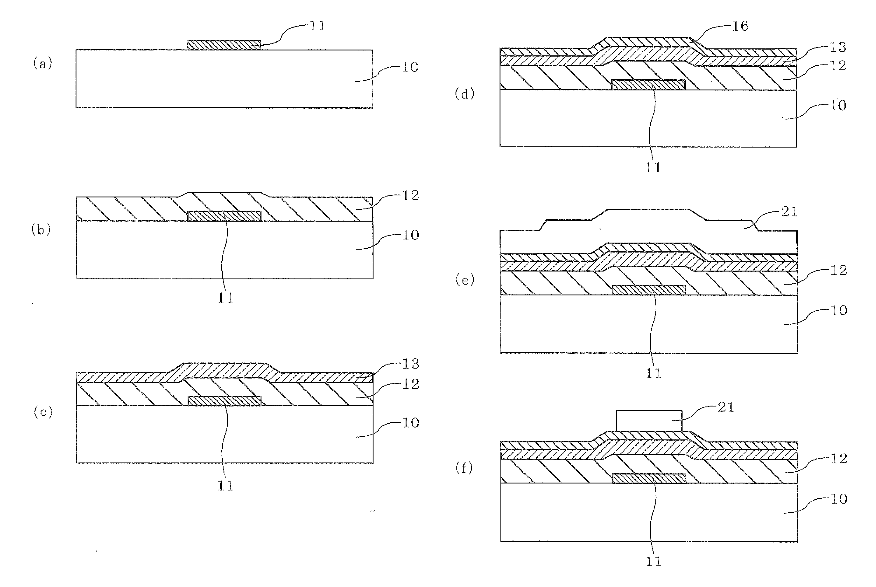
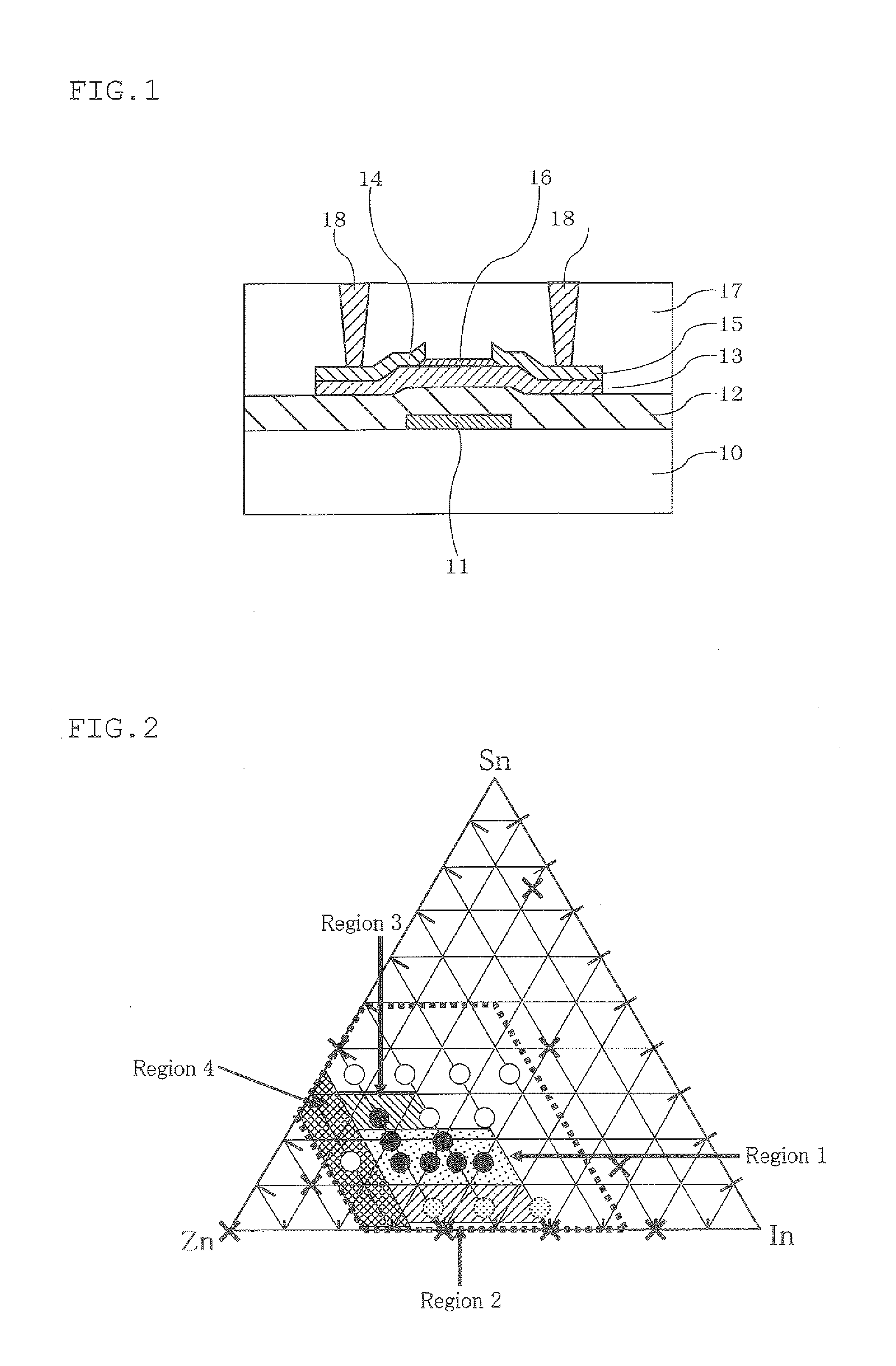
[0212]An etch-stopper (ES) type field effect transistor with a bottom-gate structure shown in FIG. 1 was fabricated. The production process will be explained below with reference to the drawings.
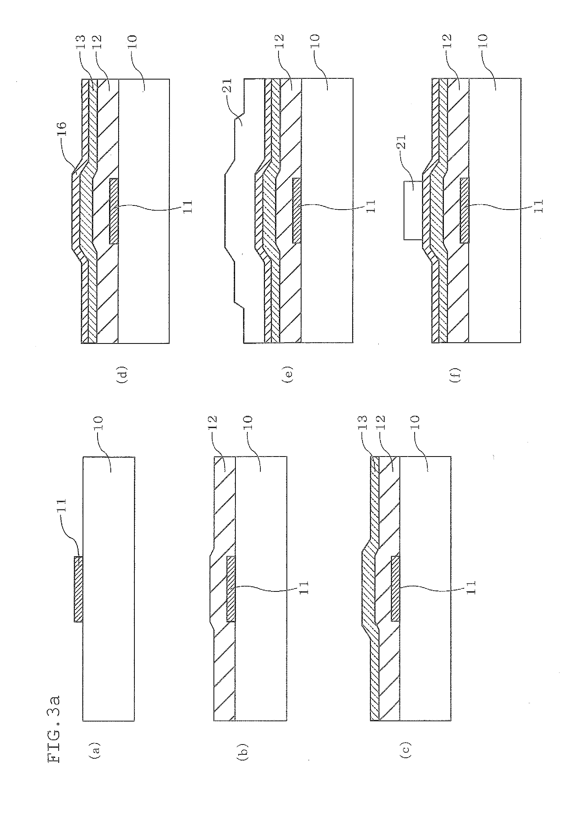
[0213]FIGS. 3a and 3b each show the steps of producing the field effect transistor.
[0214]On a glass substrate 10, metal molybdenum was formed in a thickness of 200 nm by RF sputtering at room temperature, followed by patterning by wet etching to prepare a gate electrode 11 (FIG. 3a(a)).
[0215]Next, by a plasma-enhanced chemical vapor deposition (PECVD) apparatus, SiOx was formed into a film on the substrate on which the gate electrode 11 was provided, thereby to form a gate insulating film 12 (FIG. 3a(b)).
[0216]Next, the targets for a semiconductor layer produced in Evaluation Examples 1 to 17 were mounted in a film-forming apparatus of the DC magnetron sputtering method, which is one of the DC sputtering methods, and a semiconductor layer 13 (film thickness: 30 nm) was formed on the gate ins...
examples 18 to 25
[0230]Transistors were fabricated and evaluated in the same manner as in Example 1, except that the semiconductor layer was formed at the same conditions as those in Evaluation Examples shown in Tables 4 and 5. The results are shown in Table 7.
examples 26 to 32
[0231]Transistors were fabricated and evaluated in the same manner as in Example 1, except that the formation of the semiconductor layer and the source / drain electrodes were changed as shown in Tables 4 and 5, and the formation of the semiconductor layer and the formation of the source / drain electrodes were conducted by wet etching.
[0232]The semiconductor layer was patterned by using an oxalic acid-based etching solution, and the source electrode and the drain electrode were patterned by using a PAN-based etching solution.
PUM
| Property | Measurement | Unit |
|---|---|---|
| bulk resistance | aaaaa | aaaaa |
| surface roughness | aaaaa | aaaaa |
| Feret's diameter | aaaaa | aaaaa |
Abstract
Description
Claims
Application Information
 - R&D
- Intellectual Property
- Life Sciences
- Materials
- Tech Scout
- Unparalleled Data Quality
- Higher Quality Content
- 60% Fewer Hallucinations
Browse by: Latest US Patents, China's latest patents, Technical Efficacy Thesaurus, Application Domain, Technology Topic, Popular Technical Reports.
© 2025 PatSnap. All rights reserved.Legal|Privacy policy|Modern Slavery Act Transparency Statement|Sitemap|About US| Contact US: help@patsnap.com


