
Method for deposition of high-performance coatings and encapsulated electronic devices

a technology of encapsulation and electronic devices, applied in thermoelectric devices, sustainable manufacturing/processing, final product manufacturing, etc., can solve the problems of generating substantial heat, not being effective in promoting adequate adhesion, and being expensive to use such wettabl

Active Publication Date: 2016-04-21
AIXTRON AG
View PDF2 Cites 48 Cited by
  • Summary
  • Abstract
  • Description
  • Claims
  • Application Information

AI Technical Summary

Benefits of technology

The present patent allows for the creation of durable, flexible coatings on sensitive devices that can withstand extreme weather and temperature conditions without cracking or peeling. This results in better protection and reliability for the devices.

Problems solved by technology

Where the application is very cost sensitive it may be too expensive to use such wettable polymers, and for many inexpensive plastics an inert gas treatment has been found not to be effective in promoting adequate adhesion of the hard coating.
This technique works quite well at substrate temperatures less than or about 100° C., but this technique generates substantial heat and produces films that are often not as amorphous and effective as barriers.
In some applications where the plastic or polymer substrate is thick or cannot be cooled effectively sputtering may not be acceptable due to heating of the substrate.
Plasma enhanced CVD has been used very predominantly in applications where the limiting temperature for the substrate is above about 250° C., but has not been capable of providing commercially competitive rates of deposition of high quality dielectrics at substrate temperatures under 100° C.
But there are also substantial technological challenges to be solved before AMOLED displays larger than a square decimeter—such as useful for tablet or laptop displays—can be manufactured with high yield.
In particular, the interface between low work-function metals, used for the electron emitting layer in an OLED device, and the electron transport layer are highly sensitive to damage by oxidation.
Currently this can only be done in mass production using a top covering of glass which is 100 or more microns thick.
High-vacuum chambers with such a high degree of vacuum integrity are not uncommon, but require careful design, use metal seals, are expensive to make and are not generally mass-produced.
This is an expensive technique ($50 / m2 to $100 / m2) and only suitable for relatively small and rigid displays, such as on smart phones or tablets.
This encapsulation technique also suffers from difficulty relating to stresses when front and back surfaces are not maintained at precisely the same temperature.
Finally, the double glass encapsulation method is almost inflexible, even when the glass cover is extremely thin.
This is extremely limiting since the highest value OLED displays will be those that are flexible, both because they will be lighter and less fragile, and able to made into new and compact displays that simply cannot be made with LCD technology.
Such films when they are thick enough to be robust and scratch resistant are quite brittle and do not tolerate flexure of the substrate very well.
Further, thicker conventional PECVD or PACVD layers that are more robust have poor bonding around the edges of the surface defects and during flexure of the substrate initiate microcracks around such defects where material quality is poor.
Such microcracks then propagate into the barrier layer resulting in leakage paths for moisture.
The consequent leaking of atmosphere into the sensitive material layers damages the device, making a “black spot” on the screen or lighting panel.
These are highly transparent and yet very dense dielectrics that do not permit substantial moisture permeation and can be applied by vacuum coating processes for which there is substantial production experience.
This ideally results in a wide lateral separation of the defects in successive barrier layers such that the effective path length for transmission of oxygen and water molecules is substantially increased, and a very long latency period before moisture can penetrate all layers to the device.
While very thin (<30 nm) inorganic films such as silicon dioxide and silicon nitride accommodate substantial expansion without cracking, thicker films often do crack.
Further, it would be helpful if an antireflection coating had an ability to resist scratching so that cleaning dust would not reduce the light transmission and efficiency.
There are currently no known deposition processes that can produce the coatings within the cost limits.

Method used


Image

  • Method for deposition of high-performance coatings and encapsulated electronic devices
  • Method for deposition of high-performance coatings and encapsulated electronic devices
  • Method for deposition of high-performance coatings and encapsulated electronic devices

Examples


Embodiment Construction

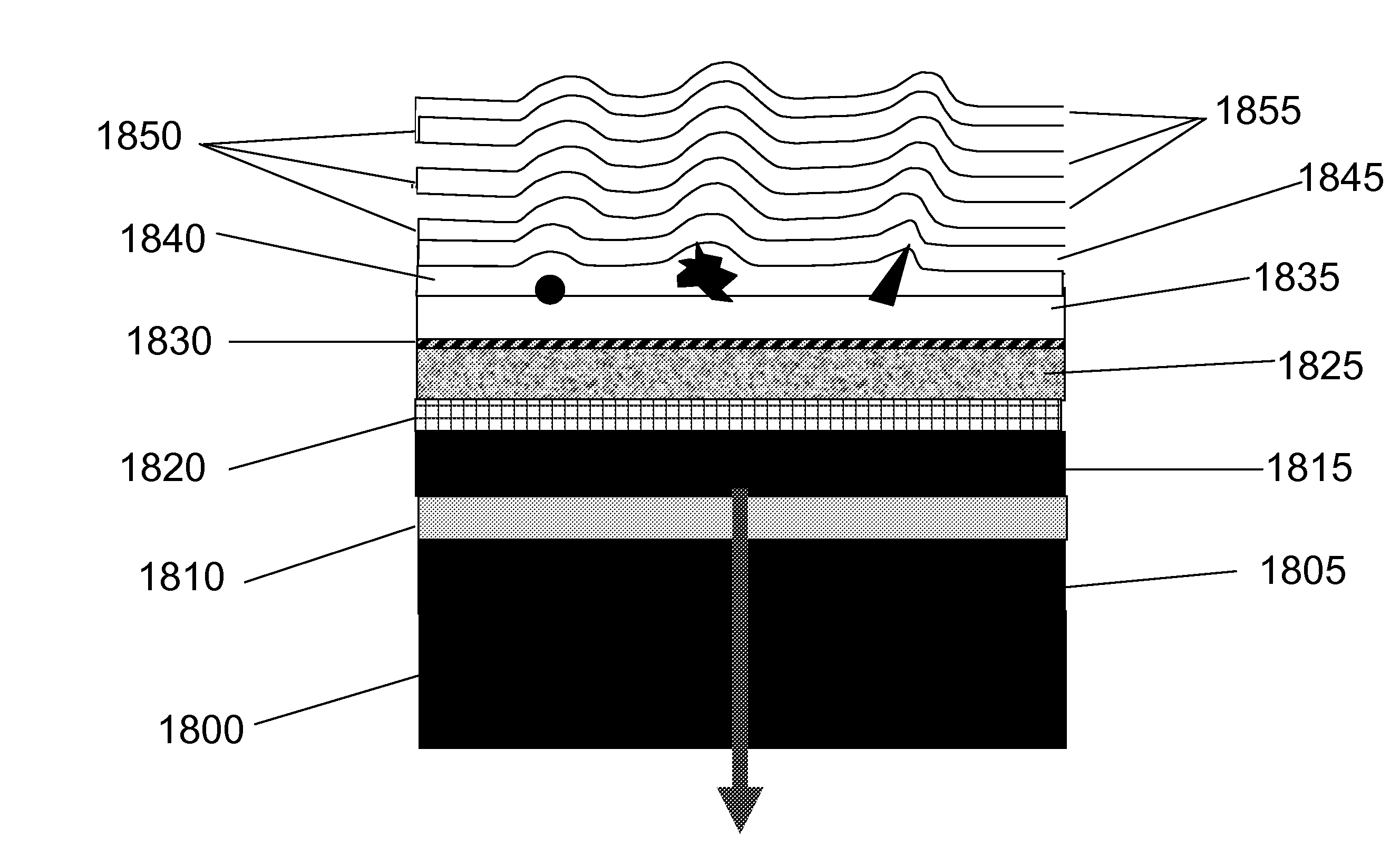
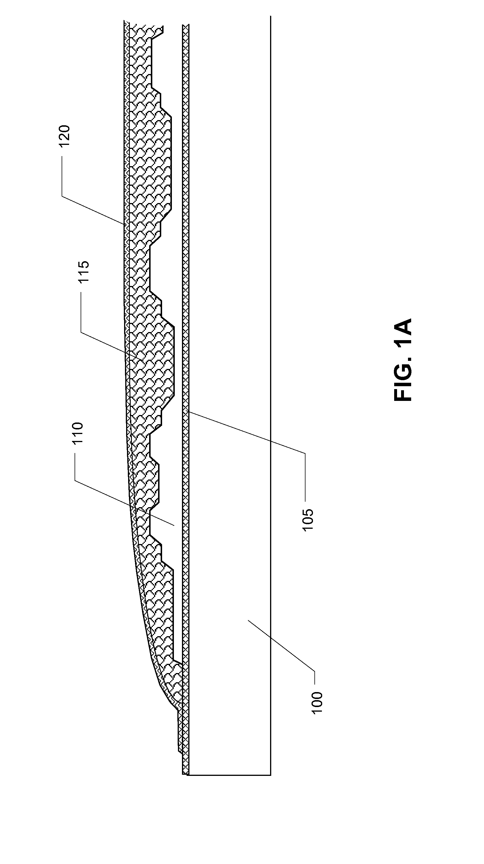
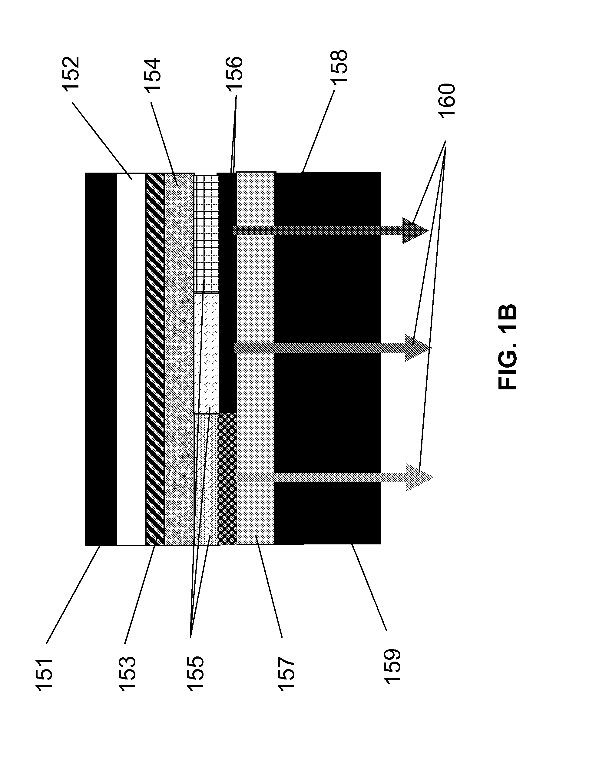
[0048]The present invention affords coatings of large substrates, continuous webs, or wafers with flexible, transparent, adherent multi-layer film structures having at least three thin layers that have one or more of the following economically important benefits:[0049]Hermetic coatings of materials and devices sensitive to air or moisture that are virtually pinhole and leak-free at highly competitive cost in mass production. Such coatings are more valuable if they are also tolerant of flexure without cracking and tolerant of very hot, moist conditions.[0050]Optical coatings of flexible plastic films that tolerate flexure and / or large temperature variations without de-lamination, micro-cracking or discoloration.[0051]Hard, protective coatings on moisture sensitive or chemically sensitive devices that can withstand outdoor or highly variable temperature conditions without cracking or peeling.

[0052]An example of an application that benefits from this method is the need for ultra low pe...


PUM

PropertyMeasurementUnit
Temperatureaaaaaaaaaa
Fractionaaaaaaaaaa
Linear densityaaaaaaaaaa

Abstract

A method is disclosed for forming multi-layered structures on polymeric or other materials that provide optical functions or protect underlying layers from exposure to oxygen and water vapor. Novel devices are also disclosed that may include both multi-layered protective structures and AMOLED display, OLED lighting or photovoltaic devices. The protective multi-layer structure itself may be made by depositing successively on a substrate at least three very thin layers of material with different density or composition. In some methods for deposition of such film, the layers are deposited by varying the energy of ion bombardment per unit thickness of the film Any layer of the structure may include one or more of the materials: silicon nitride, silicon oxide, silicon oxynitride, or metallic nitride or oxide. Specific commercial applications that benefit from this include manufacturing of photovoltaic devices or organic light emitting diode devices (OLED) including lighting and displays.

Description

RELATED APPLICATIONS[0001]This application is a utility application that claims priority benefit of U.S. Provisional Application Ser. No. 61 / 841,287 filed Jun. 29, 2013, and Provisional Application Ser. No. 61 / 976,420 filed Apr. 7, 2014; the contents of which are hereby incorporated by reference.FIELD OF THE INVENTION[0002]This invention pertains to a method for depositing high-performance coatings either as barriers to protect against penetration of oxygen and water vapor, or to provide anti-reflection or optical filtering.BACKGROUND OF THE INVENTION[0003]Thin films that protect an underlying material sensitive to moisture, oxygen and other chemicals are commonly used in many industrial processes. Applications range from food packaging, hard coatings on eyeglass lenses, and window glass, to protection of integrated circuits, display screens, and photovoltaic panels. Such thin films need to be dense, have excellent adhesion to the underlying layer and not crack or peel for the life ...

Claims


Application Information

Patent Timeline
IPC IPC(8): H01L51/52H01L51/00H01L51/56
CPCH01L51/5256H01L51/56H01L51/0097H01L2251/558H01L2251/5338H01L2251/301H01L51/5243H10K59/8731C23C16/308C23C16/345C23C16/50Y02E10/549Y02P70/50H10K50/8445H10K50/8423H10K71/00H10K77/111H10K2102/00H10K2102/311H10K2102/351
Inventor SAVAS, STEPHEN E.WIESNOSKI, ALLAN B.
Owner AIXTRON AG
Learn More