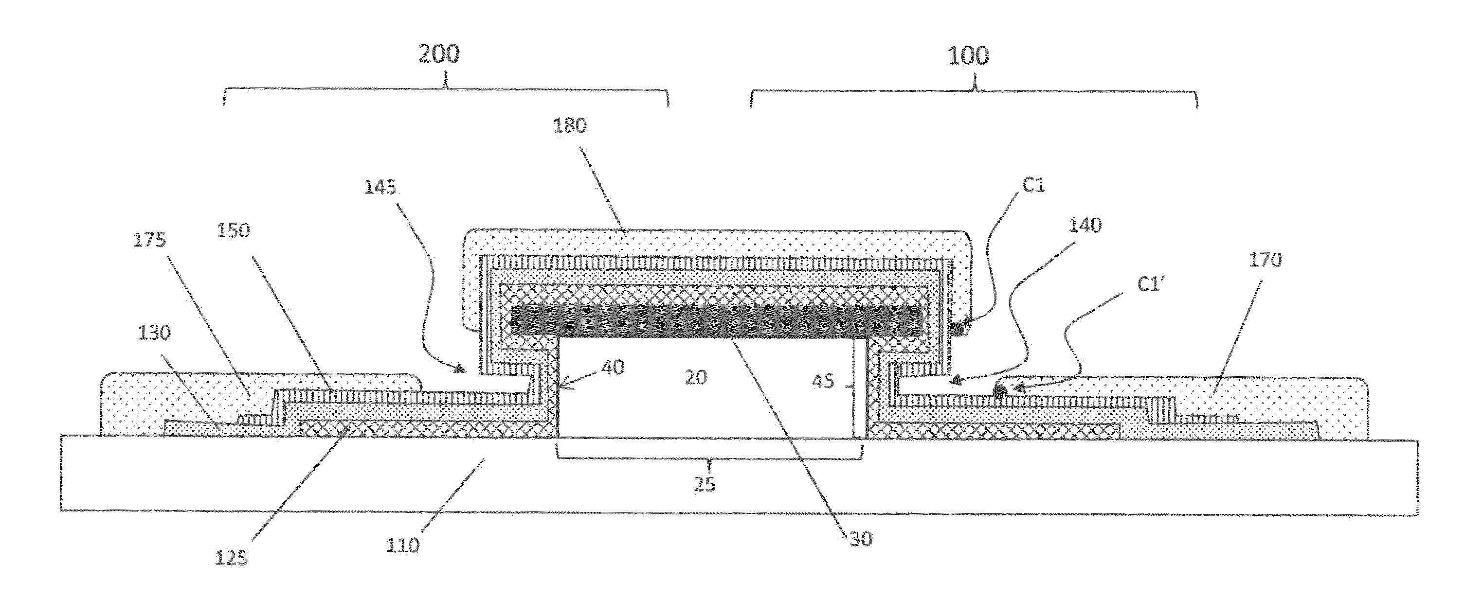
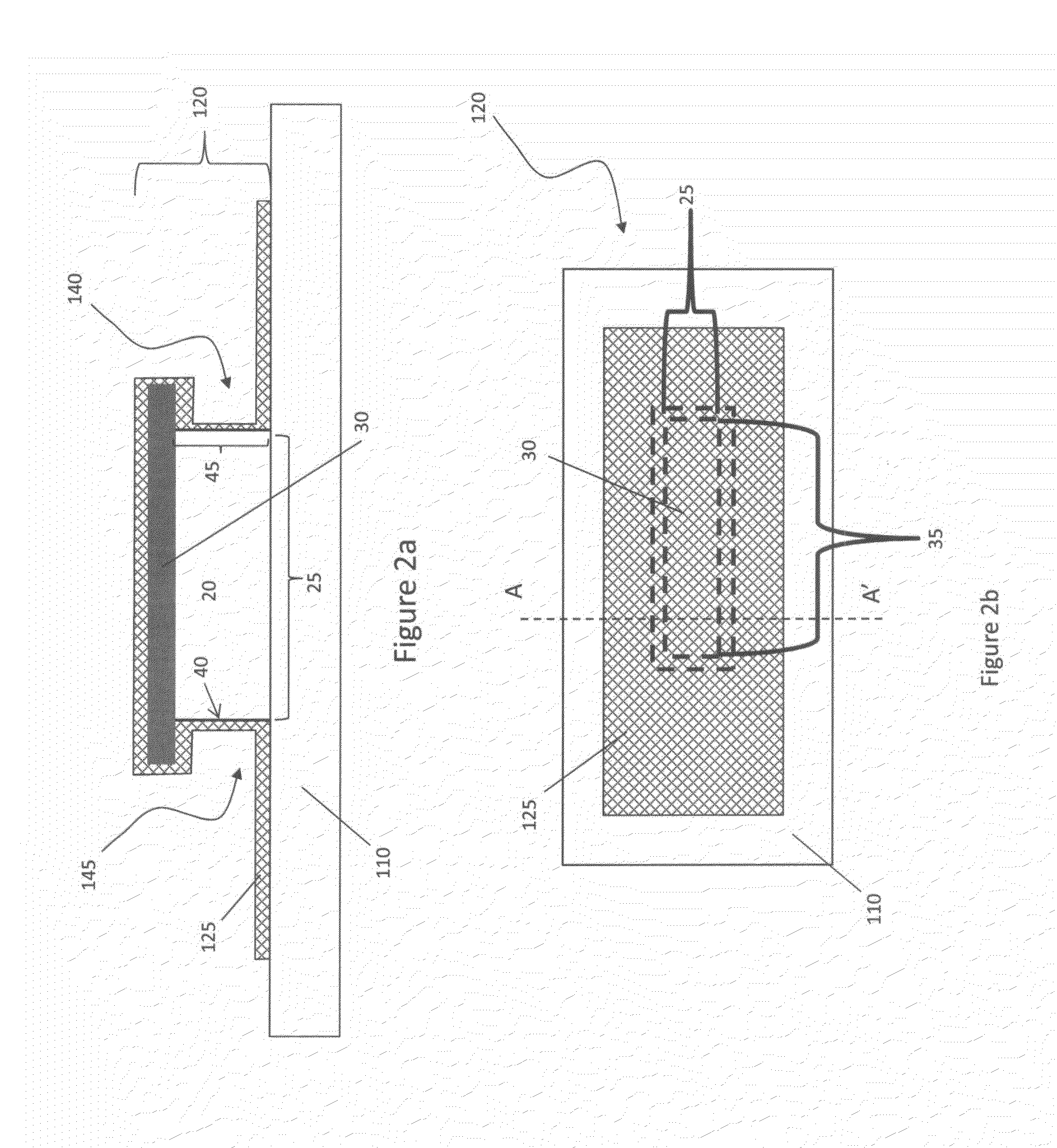
Vertically spaced electrode structure
a vertical spaced, electrode technology, applied in the direction of semiconductor/solid-state device details, coatings, printed circuit aspects, etc., can solve the problems of high cost, high quality films, limited feature size obtainable using traditional processing methods,
- Summary
- Abstract
- Description
- Claims
- Application Information
AI Technical Summary
Benefits of technology
Problems solved by technology
Method used
Image

Examples
examples
Description of the Coating Apparatus
[0164]The process of depositing the inorganic thin film layers of the following examples all employ a flow setup as described with reference to FIG. 66. The flow setup is supplied with nitrogen gas flow 81 that has been purified to remove oxygen and water contamination to below 1 ppm. The gas is diverted by a manifold to several flow meters which control flows of purge gases and of gases diverted through bubblers to select the reactive precursors. In addition to the nitrogen supply, air flow 90 is also delivered to the apparatus. The air is pretreated to remove moisture.
[0165]The following flows are delivered to the ALD coating apparatus: metal (zinc) precursor flow 92 containing metal precursors diluted in nitrogen gas; oxidizer-containing flow 93 containing non-metal precursors or oxidizers diluted in nitrogen gas; and nitrogen purge flow 95 composed only of the inert gas. The composition and flows of these streams are controlled as described be...
example i1
Inventive Example I1
Four Pixel with Printed VTFT
[0189]To fabricate Inventive Example I1, a glass substrate was provided and cleaned using an O2 plasma (100 W 0.3 Torr for 1 minute). Next, a 40 wt % solution of SU-8 2010 in cyclopentanone was spun for 10 sec at 500 rpm and ramped to a final spin of 30 sec at 2000 rpm. This coating was cured using a recipe consisting of a two minute pre-exposure hot plate bake at 95° C., 90 second blanket exposure, a two minute post-exposure hot plate bake at 95° C. and final hard bake at 225° C. for 5 minutes resulting in a 7500 Å film of cured SU-8.
[0190]Next, the surface of the SU-8 was treated with a 30 second O2 plasma to activate the surface of the SU-8. The inorganic cap was formed over the SU-8 layer using the combination of SAD and ALD. Selective area deposition was done using a patterned deposition inhibiting material layer using a Fuji Dimatix 2500 piezo-inkjet printer, as described in reference to Comparative Example C1 at the same 70 micr...
example i2
Inventive Example I2
Three Pixel with Printed VTFT Layer
[0198]Inventive Example I2 was formed using the same process, and on the same substrate, as Inventive Example I1. The only difference between Inventive Example I2 and I1, is that Inventive Example I2 had a 3 pixel wide pattern used to define the width of the transistor when forming the source and drain electrodes.
[0199]The VTFT of Inventive Example I2 is shown in FIGS. 68a through 68c. FIG. 68a is an optical micrograph of the complete VTFT. The first, second and third electrodes (180, 170 and 175) are labeled as in FIG. 1b for ease in understanding. The post and cap structure is identified by the outline of the cap 30. The optical micrograph of FIG. 68a illustrates the feature of the present invention where the channel defined by the first electrode and the second electrode including a width dimension and a length dimension, wherein the length dimension varies along the width dimension of the transistor. FIG. 68b is a SEM image ...
PUM
| Property | Measurement | Unit |
|---|---|---|
| height | aaaaa | aaaaa |
| feature size | aaaaa | aaaaa |
| thicknesses | aaaaa | aaaaa |
Abstract
Description
Claims
Application Information
 - R&D
- Intellectual Property
- Life Sciences
- Materials
- Tech Scout
- Unparalleled Data Quality
- Higher Quality Content
- 60% Fewer Hallucinations
Browse by: Latest US Patents, China's latest patents, Technical Efficacy Thesaurus, Application Domain, Technology Topic, Popular Technical Reports.
© 2025 PatSnap. All rights reserved.Legal|Privacy policy|Modern Slavery Act Transparency Statement|Sitemap|About US| Contact US: help@patsnap.com