Insulated wire having a layer containing bubbles, electrical equipment, and method of producing insulated wire having a layer containing bubbles
- Summary
- Abstract
- Description
- Claims
- Application Information
AI Technical Summary
Benefits of technology
Problems solved by technology
Method used
Image
Examples
example 1
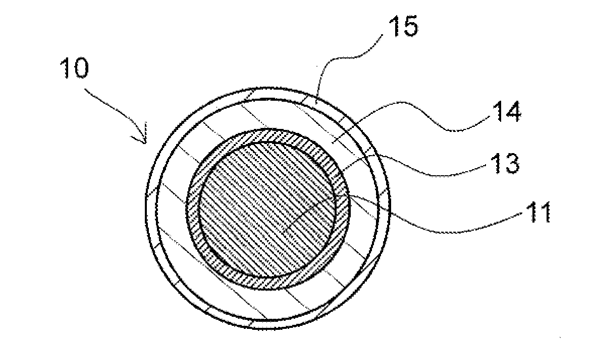
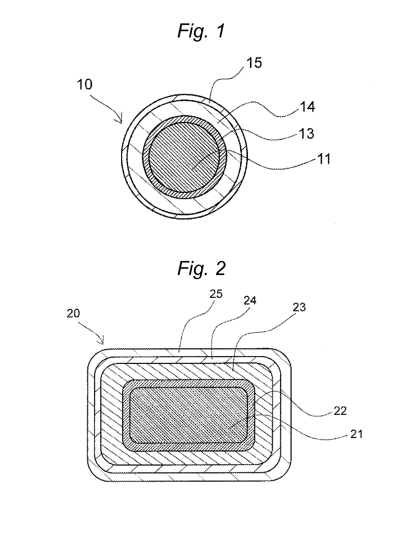
[0099]An insulated wire as shown in FIG. 1 was produced as follows.
[0100]In a 2-L separable flask, HI-406 (an NMP solution containing resin components at a proportion of 32% by mass) (trade name, manufactured by Hitachi Chemical Co., Ltd.) was introduced, and tetraethylene glycol dimethyl ether and triethylene glycol dimethyl ether were added to this solution as bubble forming agents. Thus, a varnish capable of forming bubbles was obtained.
[0101]This varnish capable of forming bubbles was applied on the outer circumference of a copper wire having a diameter of 1 mm, and baking was performed at a furnace temperature of 500° C. Thus, an insulated wire of Example 1 having a coating film which had a thickness of 32 μm and included a 2-μm layer containing no bubbles as an upper layer and a lower layer, on the outer circumference of the conductor was obtained. The bubble distribution density was 5×10¹⁰ bubbles / cm3 in the insulating film layer.
example 2
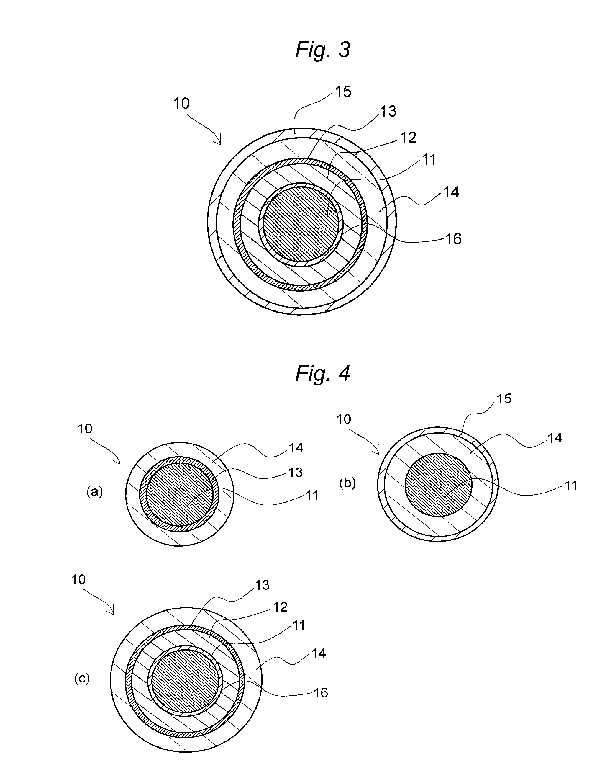
[0102]An insulated wire as shown in FIG. 4(a) was produced as follows.
[0103]In a 2-L separable flask, HI-406 (an NMP solution containing resin components at a proportion of 32% by mass) (trade name, manufactured by Hitachi Chemical Co., Ltd.) was introduced, and N,N-dimethylpropyleneurea, triethylene glycol dimethyl ether, and N-dimethylethyleneurea were added to this solution as bubble forming agents. Thus, a varnish capable of forming bubbles was obtained.
[0104]First, HI-406 (trade name, manufactured by Hitachi Chemical Co., Ltd.) containing no bubble forming agent added thereto was applied and baked on the outer circumference of a copper wire having a diameter of 1 mm, subsequently the varnish capable of forming bubbles described above was applied thereon, and baking was performed at a furnace temperature of 550° C. Thus, an insulated wire of Example 2 having a coating film having a thickness of 31 μm on the outer circumference of the conductor was obtained. The bubble distributi...
example 3
)
[0105]An insulated wire as shown in FIG. 4(b) was produced as follows. The same varnish capable of forming bubbles as that of Example 2 was applied on the outer circumference of a copper wire having a diameter of 1 mm, and baking was performed at a furnace temperature of 550° C. Furthermore, HI-406 (trade name, manufactured by Hitachi Chemical Co., ltd.) as a varnish of thermosetting resin PAI was applied with no change as an outer layer and baked. Thus, an insulated wire of Example 3 having a coating film having a thickness of 32 μm on the outer circumference of the conductor was obtained. The bubble distribution density was 4×10¹⁰ bubbles / cm3 in the insulating film layer.
PUM
| Property | Measurement | Unit |
|---|---|---|
| Thickness | aaaaa | aaaaa |
| Thickness | aaaaa | aaaaa |
| Size | aaaaa | aaaaa |
Abstract
Description
Claims
Application Information
 - R&D
- Intellectual Property
- Life Sciences
- Materials
- Tech Scout
- Unparalleled Data Quality
- Higher Quality Content
- 60% Fewer Hallucinations
Browse by: Latest US Patents, China's latest patents, Technical Efficacy Thesaurus, Application Domain, Technology Topic, Popular Technical Reports.
© 2025 PatSnap. All rights reserved.Legal|Privacy policy|Modern Slavery Act Transparency Statement|Sitemap|About US| Contact US: help@patsnap.com


