
Graphene magnetic tunnel junction spin filters and methods of making

a technology of tunnel junction and spin filter, which is applied in the field of making graphene tunnel junction spin filter and the field of graphene magnetic tunnel junction spin filter, to achieve the effect of superior properties

Inactive Publication Date: 2014-06-05
UNIVERSITY OF NORTH TEXAS
View PDF14 Cites 20 Cited by
  • Summary
  • Abstract
  • Description
  • Claims
  • Application Information

AI Technical Summary

Benefits of technology

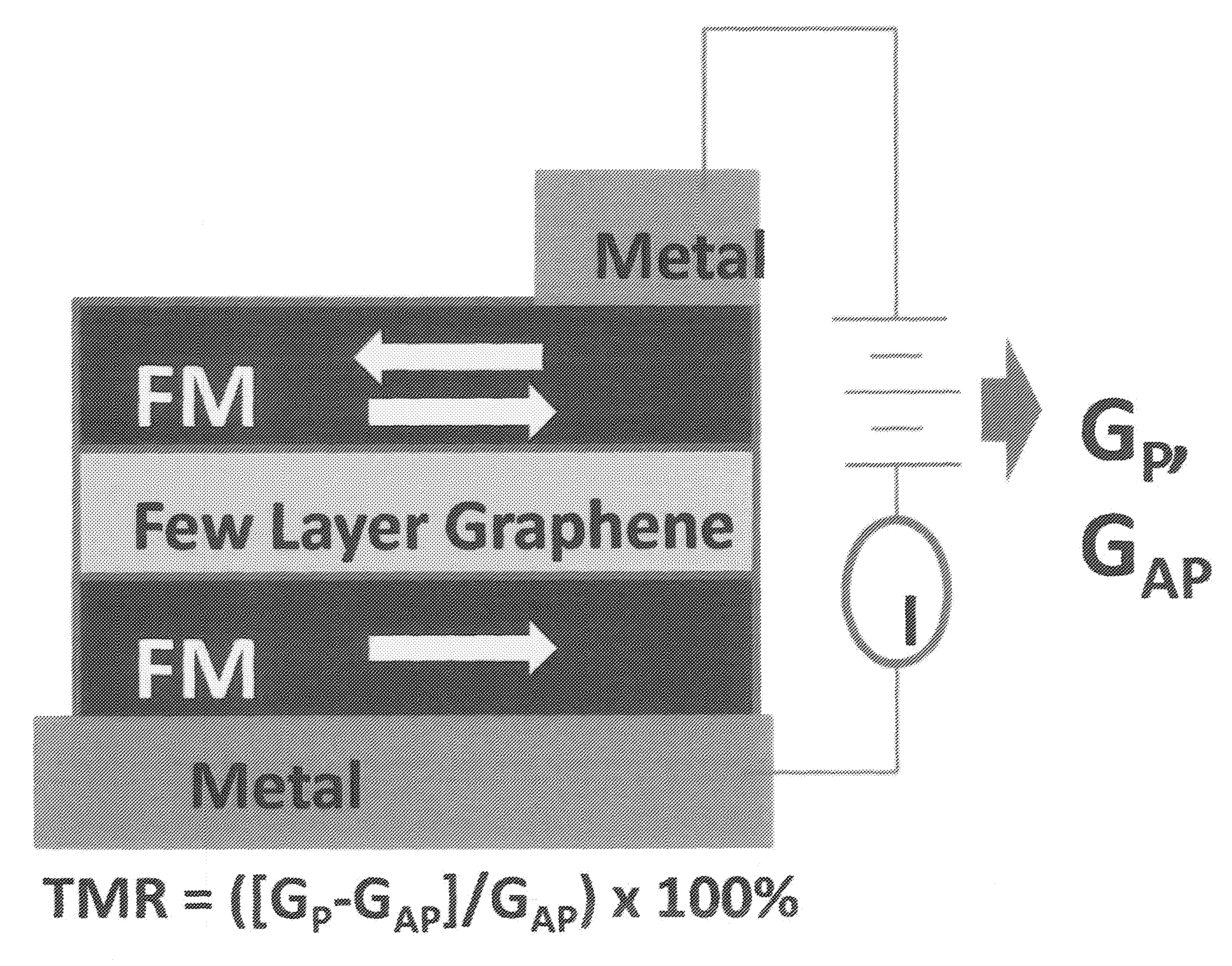
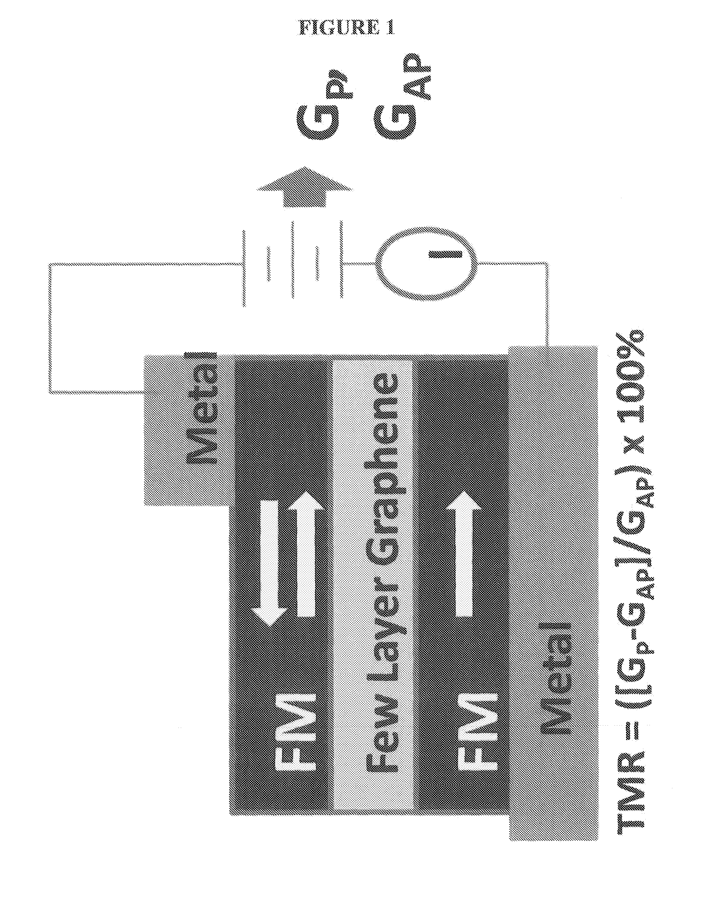
This patent describes a way to create a thin layer of graphene directly on top of a layer of cobalt or nickel on copper interconnects in a way that is compatible with the requirements of silicon CMOS fabrication. This graphene layer can then be used to create an MTJ, which is useful for the development of non-volatile memory. By doing this, researchers have been able to create a superior MTJ that has properties that are advantageous for the use of such memory.

Problems solved by technology

Loss of optimum MTJ performance parameters aside, the processing temperatures involved for these and other graphene films formed by CVD (>750 K) pose significant problems for integration with Si CMOS at the interconnect or packaging levels.

Method used


Image

  • Graphene magnetic tunnel junction spin filters and methods of making
  • Graphene magnetic tunnel junction spin filters and methods of making
  • Graphene magnetic tunnel junction spin filters and methods of making

Examples


Embodiment Construction

Procedures and Results

[0014]The FM / few layer graphene / FM stack based MTJ of the invention was made by first using electron beam evaporation to deposit ˜40 Å of (disordered) cobalt on a Al2O3 (0001) substrate, at a background pressure of ˜1×10⁻⁸ Torr, resulting in some carbon being dissolved in the cobalt film. Annealing of the film to ˜600 K in UHV results in the segregation of dissolved carbon to the surface of the cobalt film as it orders to form a Co(111) film with carbon overlayer.

[0015]Auger C(KVV) Auger data (FIG. 2) shows that the thickness of the carbon overlayer grows to an average thickness of ˜3.5 monolayers during the annealing process, while transforming from sp3 to sp2 carbon chemical bonding—the formation of few layer graphene.

[0016]Corresponding LEED data (FIG. 3) obtained from the carbon segregation event demonstrate that the graphene layers are highly ordered, displaying well-defined diffraction spots at 300 relative to the Co diffraction spots. The Auger data (FIG...


PUM

PropertyMeasurementUnit
temperaturesaaaaaaaaaa
thicknessaaaaaaaaaa
temperaturesaaaaaaaaaa

Abstract

A Tunnel Magnetic Junction of high magnetoresistance is prepared at temperatures and pressure consistent with Si CMOS fabrication and operation. A first metal layer of cobalt or nickel is grown on an interconnect or conductive array line of e.g., copper. The metal layer is formed by electron beam irradiation. Annealing at UHV at temperatures below 700K yields a carbon segregation that forms a few layer thick (average density 3.5 ML) graphene film on the metal layer. Formation of a second layer of metal on top of the graphene barrier layer yields a high performance MTJ.

Description

PRIORITY DATA AND INCORPORATION BY REFERENCE[0001]This application claims benefit of priority to U.S. Provisional Patent Application No. 61 / 490,650 filed May 27, 2011 which is incorporated by reference in its entirety.FIELD OF THE INVENTION[0002]The present invention relates to methods of forming a few molecule thick (1-3 or 4 monolayer) graphene layer on a ferromagnetic layer, at temperatures and conditions consistent with integration with silicon-based complementary metal oxide semiconductors (Si CMOS). Specifically, this invention permits for the first time the manufacture of magnetic tunnel junction spin filters and related devices based on graphene on Si CMOS devices at temperatures and conditions consistent with those preexisting structures.BACKGROUND OF THE INVENTION[0003]The increasing demand for high density magnetic recording and playback, and requirements for non-volatile memory, have focused attention on magnetic tunnel junctions, and the devices that can be prepared the...

Claims


Application Information

Patent Timeline
Patent Type & Authority Applications(United States)
IPC IPC(8): H01L43/08H01L21/02H10N50/01H10N50/10
CPCH01L21/0237H01L43/08C01B2204/04H01L21/0242H01L21/02433H01L21/02491H01L21/02516H01L21/02527H01L21/02631H01L21/02664C01B32/184G11C11/161H10B61/00H10N50/01H10N50/85H10N50/10G11C11/15H01L21/0262
Inventor KELBER, JEFFRYZHOU, MI
Owner UNIVERSITY OF NORTH TEXAS
Learn More