
Conductive paste composition and semiconductor devices made therewith

a technology of conductive paste and composition, which is applied in the direction of electrically conductive paint, conductor, metal/alloy conductor, etc., can solve the problems of increasing recombination losses that reduce both current and voltage of the cell, solar cell energy loss, and voc (open circuit voltage) and isc (short circuit current)

Active Publication Date: 2014-03-06
SOLAR PASTE LLC
View PDF2 Cites 9 Cited by
  • Summary
  • Abstract
  • Description
  • Claims
  • Application Information

AI Technical Summary

Benefits of technology

The patent relates to a paste composition that can be used to form electrically conductive structures on a substrate. The composition includes a source of electrically conductive metal, an alkaline-earth-metal boron tellurium oxide, and an organic vehicle in which the metal and oxide are dispersed. The composition may also contain a small amount of a discrete oxide additive or a metal or compound that generates an oxide upon firing. The process involves applying the paste to the substrate and firing it to form the conductive structure. This process can be used to create high-quality electrically conductive structures such as semiconductor devices and photovoltaic cells.

Problems solved by technology

However, a high dopant concentration also introduces crystalline defects or electrical perturbations in the Si lattice that increase recombination losses that reduce both the current and voltage of the cell.
The solar cell energy loss results from a decrease of both Voc (open circuit voltage) and Isc (short circuit current).
However, the inherent potential of LDE-based cells to provide improved cell performance is frequently mitigated in practice by the greater difficulty of forming the high-quality metal contacts needed to efficiently extract current from the operating cell.
The high [Psurface] emitters enable formation of low contact resistivity metallization contacts, without which contact is poor and cell performance is degraded.

Method used


Image

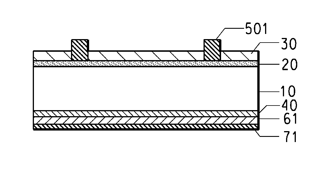
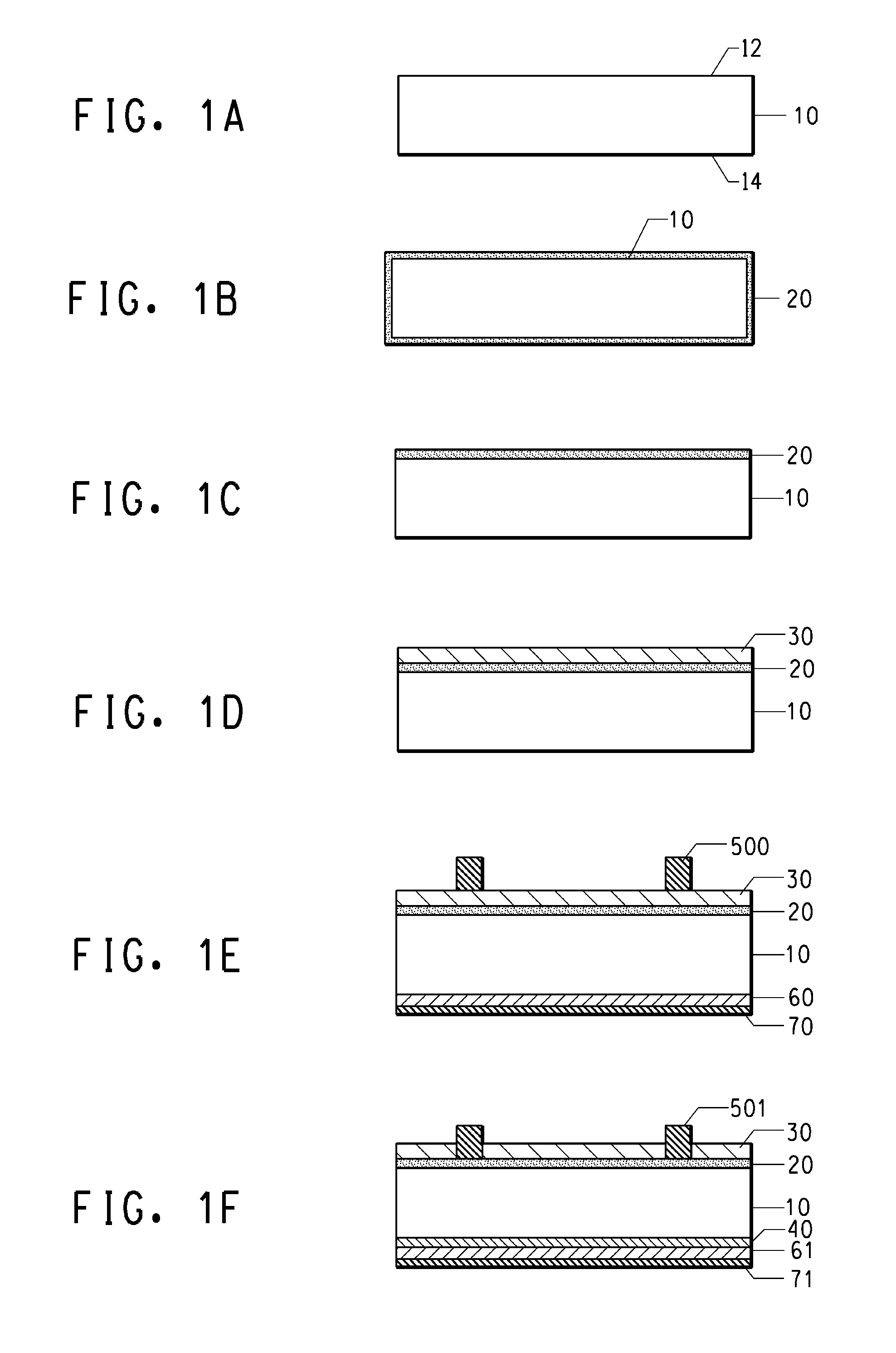
  • Conductive paste composition and semiconductor devices made therewith
  • Conductive paste composition and semiconductor devices made therewith

Examples


examples

[0199]The operation and effects of certain embodiments of the present invention may be more fully appreciated from a series of examples (Examples 1-189) described below. The embodiments on which these examples are based are representative only, and the selection of those embodiments to illustrate aspects of the invention does not indicate that materials, components, reactants, conditions, techniques and / or configurations not described in the examples are not suitable for use herein, or that subject matter not described in the examples is excluded from the scope of the appended claims and equivalents thereof.

examples 1a to 15a

Paste Preparation

[0200]In accordance with the present disclosure, a series of alkaline-earth-metal boron tellurium oxide materials was prepared. The compositions set forth in Table I were formulated by combining requisite amounts of the oxides or carbonates of Ba, Ca, Mg, Bi, Te, Li, B, Si, and Zn. The amount of each oxide or carbonate was selected to provide in the combined alkaline-earth-metal boron tellurium oxide the cation percentages listed in Table I.

[0201]The various ingredients for each composition were intimately mixed by melting them in a covered Pt crucible that was heated in air from room temperature to 1000° C. over a period of 1 hour, and held at the respective temperature for 30 minutes. Each melt was separately poured onto the flat surface of a cylindrically-shaped stainless steel block (8 cm high, 10 cm in diameter). The cooled buttons were pulverized to a −100 mesh coarse powder.

[0202]Then the coarse powder was ball milled in a polyethylene container with zirconia...

examples 1b to 15b

Fabrication and Testing of Photovoltaic Cells

Cell Fabrication

[0208]Photovoltaic cells were fabricated in accordance with an aspect of the invention using the paste compositions of Examples 1a to 15a to form the front-side electrodes for the cells of Examples 1b to 15b, respectively. The amount of frit (in wt. % based on the total paste composition) in each example is listed in Table III below.

[0209]Conventional Deutsche Cell HDE multi-crystalline wafers (˜200 μm thick, ˜65 ohms per square resistivity) were used for fabrication and electrical testing. For convenience, the experiments were carried out using 28 mm×28 mm “cut down” wafers prepared by dicing 156 mm×156 mm starting wafers using a diamond wafering saw. The test wafers were screen printed using an AMI-Presco (AMI, North Branch, N.J.) MSP-485 screen printer, first to form a full ground plane back-side conductor using a conventional Al-containing paste, SOLAMET® PV381 (available from DuPont, Wilmington, Del.), and thereafter ...


PUM

PropertyMeasurementUnit
Percent by massaaaaaaaaaa
Weightaaaaaaaaaa
Electrical conductivityaaaaaaaaaa

Abstract

A conductive paste composition contains a source of an electrically conductive metal, an alkaline-earth-metal boron tellurium oxide, and an organic vehicle. An article such as a high-efficiency photovoltaic cell is formed by a process of deposition of the paste composition on a semiconductor device substrate (e.g., by screen printing) and firing the paste to remove the organic vehicle and sinter the metal and establish electrical contact between it and the device.

Description

CROSS-REFERENCE TO RELATED APPLICATION[0001]This application claims benefit of U.S. Provisional Patent Application Ser. No. 61 / 697,463, filed Sep. 6, 2012 and entitled “Conductive Paste Composition and Semiconductor Devices Made Therewith,” which is incorporated herein in its entirety by reference thereto.FIELD OF THE INVENTION[0002]The present invention relates to a conductive paste composition that is useful in the construction of a variety of electrical and electronic devices, and more particularly to a paste composition useful in creating conductive structures, including front-side electrodes for photovoltaic devices.TECHNICAL BACKGROUND OF THE INVENTION[0003]A conventional photovoltaic cell incorporates a semiconductor structure with a junction, such as a p-n junction formed with an n-type semiconductor and a p-type semiconductor. More specifically, Si solar cells are typically made by adding controlled impurities (called dopants) to purified Si. Different dopants result in eit...

Claims


Application Information

Patent Timeline
IPC IPC(8): H01L31/0224H01B1/02
CPCH01B1/02H01L31/022408H01B1/22H01L31/022441C03C3/064C03C3/14C03C3/15C03C8/02C03C8/04C03C8/18Y10T29/49163Y02E10/50C03C3/00C09D5/24H01L31/022425H05K3/1283
Inventor LI, ZHIGANG RICKMIKESKA, KURT RICHARDROACH, DAVID HERBERTTORARDI, CARMINEVERNOOY, PAUL DOUGLAS
Owner SOLAR PASTE LLC
Learn More