
Patterning process and resist composition

Active Publication Date: 2013-02-28
SHIN ETSU CHEM IND CO LTD
View PDF0 Cites 12 Cited by
  • Summary
  • Abstract
  • Description
  • Claims
  • Application Information

AI Technical Summary

Benefits of technology

The patent describes a method for creating images using a photoresist film made of a specific polymer, a compound, and an acid generator. The film has a high dissolution contrast between unexposed and exposed regions, allowing for controlled and sensitive hole pattern formation when exposed to radiation and developed in an organic solvent. The technical effect is the ability to create high-quality and precise images using a simple and effective method.

Problems solved by technology

However, for the reasons that the projection lens uses a large amount of expensive CaF2 single crystal, the scanner thus becomes expensive, hard pellicles are introduced due to the extremely low durability of soft pellicles, the optical system must be accordingly altered, and the etch resistance of resist is low; the development of F2 lithography was stopped and instead, the ArF immersion lithography was introduced.
As compared with the line pattern, the hole pattern is difficult to reduce the feature size.
This, however, results in the exposure margin being extremely narrowed.
However, there is a problem that control accuracy becomes lower as the pattern size after development and the size after shrinkage differ greater and the quantity of shrinkage is greater.
With the hole shrinking method, the hole size can be shrunk, but the pitch cannot be narrowed.
Although a hole pattern can be formed at a wide margin by combining X and Y lines and using dipole illumination featuring a high contrast, it is difficult to etch vertically staged line patterns at a high dimensional accuracy.
However, the crosslinking negative resist film has the drawback that the resolving power is low as compared with the positive resist film, because the maximum resolution of ultrafine holes is determined by the bridge margin.

Method used


Image

  • Patterning process and resist composition
  • Patterning process and resist composition
  • Patterning process and resist composition

Examples


example

[0156]Examples of the invention are given below by way of illustration and not by way of limitation. The abbreviation “pbw” is parts by weight. For all polymers, Mw and Mn are determined by GPC versus polystyrene standards using tetrahydrofuran solvent. For measurement of the hole size of a pattern, a top-down scanning electron microscope (TDSEM) S-9380 (Hitachi High Technologies Corp.) was used.

synthesis example

[0157]Various polymers (Resist Polymers 1 to 10, Comparative Resist Polymer 1, and Blending Resist Polymers 1, 2) for use in resist compositions were prepared by combining suitable monomers, effecting copolymerization reaction in tetrahydrofuran solvent, pouring into methanol for crystallization, repeatedly washing with hexane, isolation, and drying. The polymers were analyzed by 1H-NMR to determine their composition and by GPC to determine Mw and dispersity Mw / Mn.


PUM


Abstract

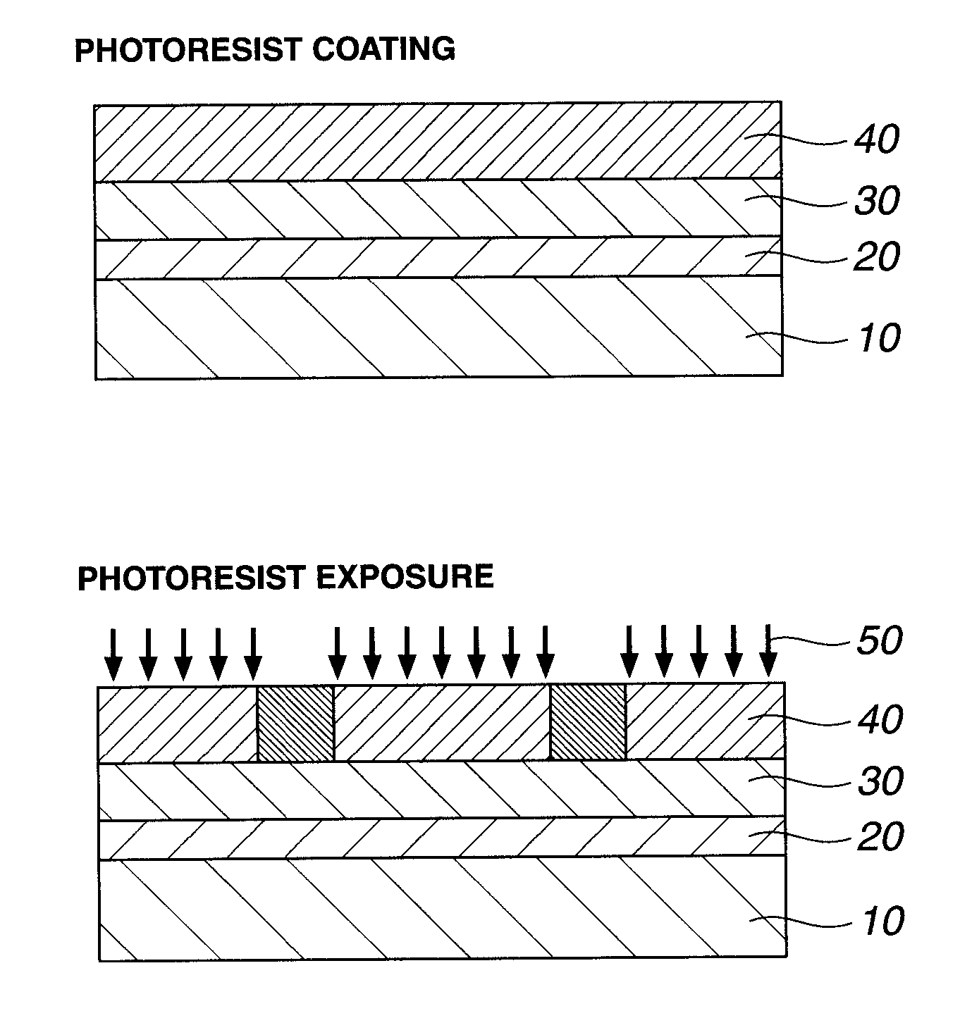
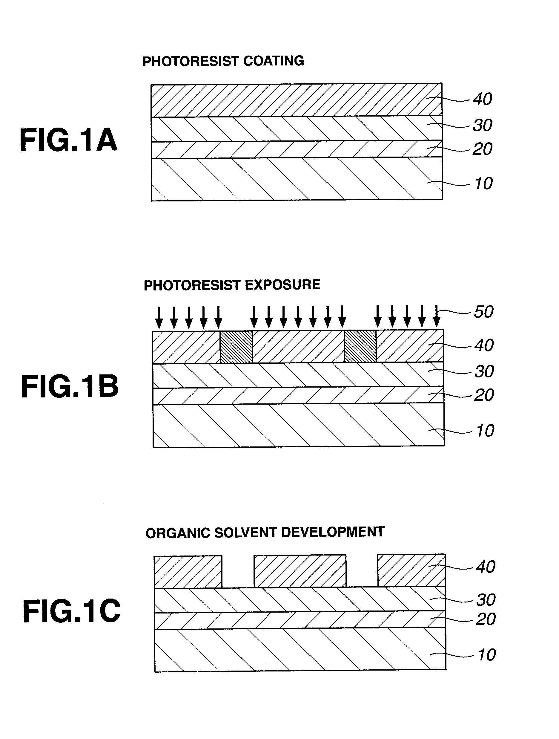
A negative pattern is formed by coating a resist composition comprising a methylol-substituted urea, amide or urethane compound, a polymer comprising recurring units having an acid labile group-substituted hydroxyl group, and an acid generator onto a substrate, prebaking, exposing to high-energy radiation, and developing in an organic solvent developer such that the unexposed region of resist film is dissolved away and the exposed region of resist film is not dissolved. In image formation via positive / negative reversal by organic solvent development, the resist film is characterized by a high dissolution contrast between the unexposed and exposed regions.

Description

CROSS-REFERENCE TO RELATED APPLICATION[0001]This non-provisional application claims priority under 35 U.S.C. §119(a) on Patent Application No. 2011-184706 filed in Japan on Aug. 26, 2011, the entire contents of which are hereby incorporated by reference.TECHNICAL FIELD[0002]This invention relates to a pattern forming process involving exposure of resist film, deprotection reaction with the aid of acid and heat, and development with an organic solvent to form a negative tone pattern in which the unexposed region is dissolved and the exposed region is not dissolved. It also relates to a resist composition used therein.BACKGROUND ART[0003]In the recent drive for higher integration and operating speeds in LSI devices, the pattern rule is made drastically finer. The photolithography which is currently on widespread use in the art is approaching the essential limit of resolution determined by the wavelength of a light source. As the light source used in the lithography for resist pattern ...

Claims


Application Information

Patent Timeline
IPC IPC(8): G03F7/20G03F7/027G03F7/004
CPCG03F7/004G03F7/0046G03F7/0382G03F7/325G03F7/0045G03F7/0397G03F7/70466Y10S430/1055
Inventor HATAKEYAMA, JUNKATAYAMA, KAZUHIROKOBAYASHI, TOMOHIRO
Owner SHIN ETSU CHEM IND CO LTD
Learn More