Grain boundary-insulated semiconductor ceramic, semiconductor ceramic capacitor, and method for producing semiconductor ceramic capacitor

a technology of grain boundary insulation and semiconductor ceramic, which is applied in the direction of fixed capacitors, conductive materials, electrical equipment, etc., can solve the problems of difficult to sufficiently oxidize crystal grain boundaries, decrease in electrical properties, and decrease in the diffusion power of grain boundary insulating agents during heat treatment, etc., to achieve good electrical properties, good practical use effect, good electrical properties

Active Publication Date: 2012-08-30
MURATA MFG CO LTD
View PDF3 Cites 5 Cited by
  • Summary
  • Abstract
  • Description
  • Claims
  • Application Information

AI Technical Summary

Benefits of technology

[0013]The inventor of the present invention has conducted intensive studies in order to achieve the above object. As a result, it was found that, by using a material free of Pb, such as a Bi—Cu-based material, as a grain boundary insulating agent and using a SiO2—X2O-MO—TiO2-based glass material that does not contain B or Pb (where X represents an alkali metal and M represents at least one element selected from Ba, Sr, and Ca) as a glass component, a grain boundary-insulated semiconductor ceramic having good electrical properties can be obtained without decreasing the insulation resistance or the breakdown voltage, even though the diffusing agent is composed of a non-Pb material.
[0023]In a grain boundary-insulated semiconductor ceramic according to a preferred embodiment of the present invention, the grain boundary insulating agent is composed of a material free of Pb, such as a Bi—Cu-based material, and the glass component contains, as a main component, a SiO2—X2O-MO—TiO2-based glass material that does not contain B or Pb (where X represents an alkali metal such as Li, and M represents at least one element selected from Ba, Sr, and Ca), and the content of the glass component is 3 to 15 parts by weight relative to 100 parts by weight of the grain boundary insulating agent. Accordingly, even though Pb is notpresent, it is possible to obtain a grain boundary-insulated semiconductor ceramic having electrical properties equal to or better than those in the case where a Pb-based diffusing agent is used, without causing a decrease in the insulation resistance or the breakdown voltage.
[0025]Furthermore, the component base is formed so as to have a tubular shape, and an electrode is formed on each of the inner peripheral surface and the outer peripheral surface of the component base, and thus the diffusing agent is uniformly or substantially uniformly distributed over the entire component base. Therefore, even in the case where the component base has a large wall thickness, it is possible to obtain a semiconductor ceramic capacitor that has good electrical properties, such as electrostatic capacity, insulation resistance, and breakdown voltage and that is excellent in terms of practical use.
[0026]The method for producing a semiconductor ceramic capacitor according to a preferred embodiment of the present invention includes the steps of preparing a sintered body by mixing a plurality of ceramic raw materials including at least a strontium compound and a titanium compound and firing the resulting mixture in a reducing atmosphere, weighing (providing) a grain boundary insulating agent composed of a material free of lead and a glass component composed of a SiO2—X2O-MO—TiO2-based glass material that does not contain boron or lead (where X represents an alkali metal, and M represents at least one of barium, strontium, and calcium), and preparing a component base by performing a heat treatment in an air atmosphere while mixing and stirring the sintered body with the grain boundary insulating agent and the glass component. Accordingly, the diffusing agent containing the grain boundary insulating agent and the glass component has a diffusing power substantially the same as that of a lead-based diffusing agent. Therefore, even when the sintered body has a tubular shape with a large wall thickness, the diffusing agent can be uniformly or substantially uniformly distributed in the component base. Thus, grain boundaries can be uniformly oxidized, and a desired grain boundary insulating layer can be formed. The semiconductor ceramic capacitor obtained has good electrical properties such as electrostatic capacity, insulation resistance, and breakdown voltage, and is excellent in terms of practical use.

Problems solved by technology

The content of Pb3O4 is small but when the Pb3O4 is removed from the grain boundary insulating agent, the diffusing power of the grain boundary insulating agent decreases during heat treatment and it becomes difficult to sufficiently oxidize crystal grain boundaries.
In particular, the grain boundary insulating agent does not sufficiently thermally diffuse in a semiconductor ceramic capacitor having a tubular shape such as a circular tube or a rectangular tube and having a large wall thickness into the inside of the capacitor, which may result in a decrease in electrical properties.
When B is incorporated in the glass component, although the effect of increasing the diffusing power can be obtained to a certain degree, the insulation resistance and the breakdown voltage tend to decrease, which may result in a decrease in electrical properties.

Method used


Image

  • Grain boundary-insulated semiconductor ceramic, semiconductor ceramic capacitor, and method for producing semiconductor ceramic capacitor
  • Grain boundary-insulated semiconductor ceramic, semiconductor ceramic capacitor, and method for producing semiconductor ceramic capacitor
  • Grain boundary-insulated semiconductor ceramic, semiconductor ceramic capacitor, and method for producing semiconductor ceramic capacitor

Examples


example 1

Preparation of Grain Boundary Insulating Agents and Glass Components

[0068]As insulating raw materials, Bi2O3, CuO, and Pb3O4 were prepared. These insulating raw materials were mixed and prepared so as to have the component compositions shown in Table 1. Thus, grain boundary insulating agents A to E were prepared.

TABLE 1Type of grainboundaryComponent composition (wt %)insulating agentBi2O3CuOPb3O4A 8515—B 9010—C 955—D 982—E*47.5547.5*Out of the range of the present invention

[0069]As is apparent from Table 1, grain boundary insulating agents A to D contain Bi2O3 and CuO and do not contain Pb3O4. Accordingly, grain boundary insulating agents A to D are grain boundary insulating agents within the range of the present invention.

[0070]In contrast, grain boundary insulating agent E contains 47.5% by weight of Pb3O4. Accordingly, grain boundary insulating agent E is a grain boundary insulating agent outside of the range of the present invention.

[0071]Next, as glass raw materials, SiO2, Li2O...

example 2

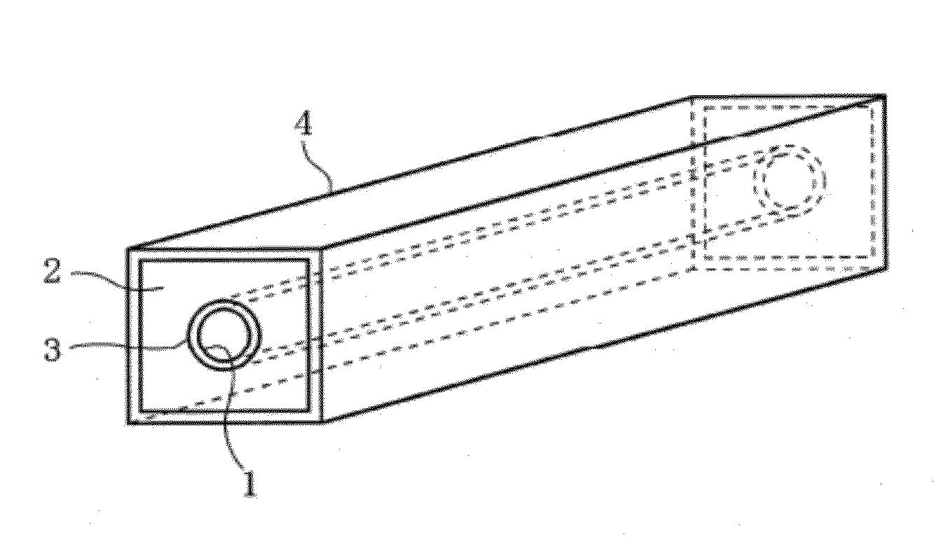
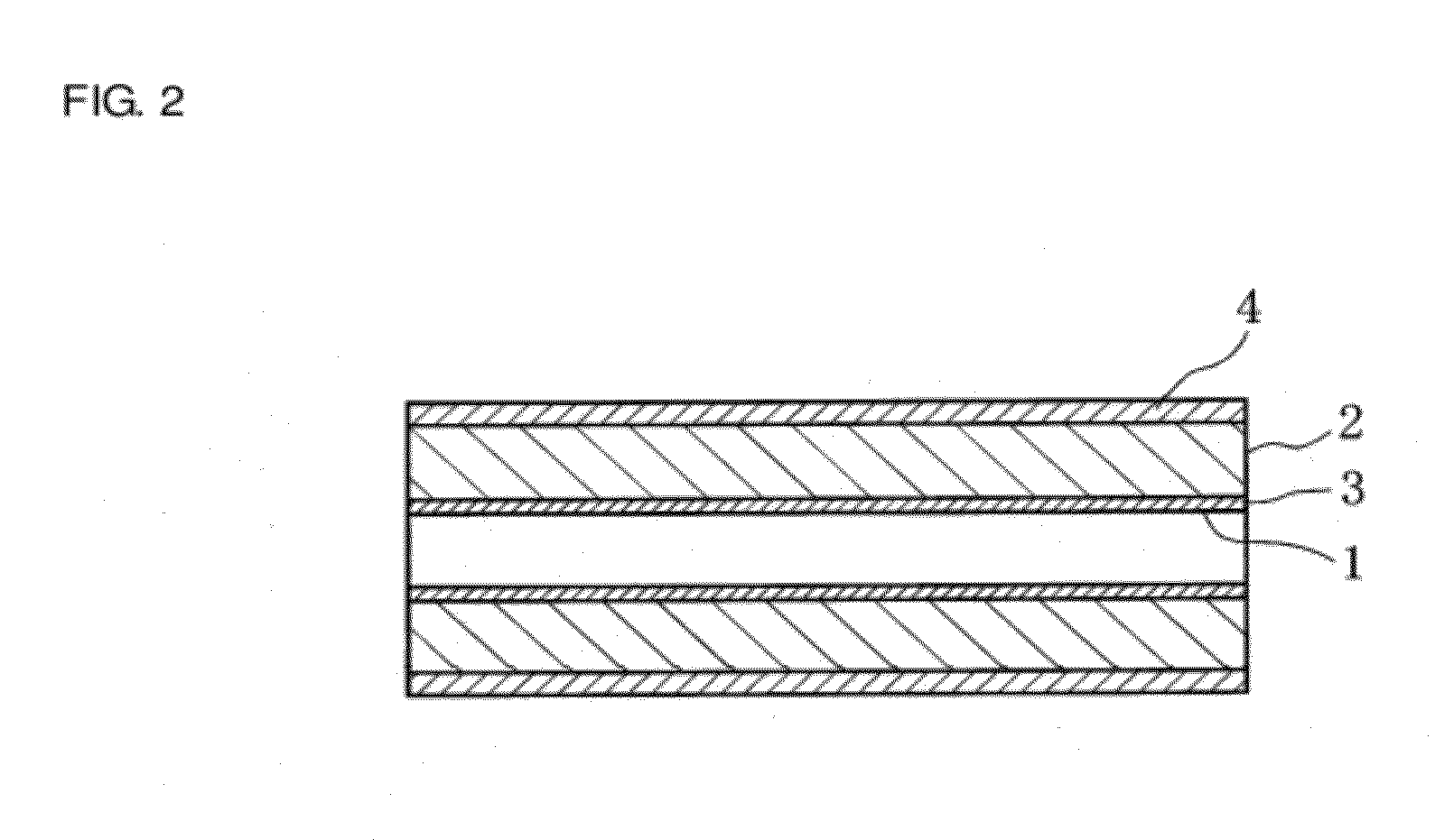
[0090]Slurries were prepared as in Example 1. Next, each of these slurries was charged in a shaping die having a predetermined shape, formed so as to have a tubular shape using an extruder, and dried in a dryer. Subsequently, the dried tube was cut to have a circular tube shape. Thus, a formed body was obtained. Thereafter, a sintered body having a circular tube shape was obtained by the same method and procedure as in Example 1. The sintered body had an outer diameter of 3.0 mm, an inner diameter of 1.6 mm, and a length of 2.5 mm.

[0091]Next, diffusing agents were prepared by mixing 0 to 15 parts by weight of one of glass components a to d with 100 parts by weight of one of grain boundary insulating agents A to E.

[0092]Each of the diffusing agents was weighed so that the amount of diffusing agent was 1.0 part by weight relative to 100 parts by weight of the sintered body having the circular tube shape. The diffusing agent was placed in an alumina sagger having a cylindrical shape to...


PUM

PropertyMeasurementUnit
wall thicknessaaaaaaaaaa
molar ratioaaaaaaaaaa
temperatureaaaaaaaaaa

Abstract

A grain boundary-insulated semiconductor ceramic contains a SrTiO3-based compound as a main component, and a diffusing agent containing a grain boundary insulating agent and a glass component. The grain boundary insulating agent is composed of a material free of lead, the glass component mainly contains a SiO2—X2O-MO—TiO2-based glass material that does not contain boron or lead and in which X represents an alkali metal, and M represents at least one of barium, strontium, and calcium, and the content of the glass component is 3 to 15 parts by weight relative to 100 parts by weight of the grain boundary insulating agent. A component base is composed of the grain boundary-insulated semiconductor ceramic.

Description

BACKGROUND OF THE INVENTION[0001]1. Field of the Invention[0002]The present invention relates to a grain boundary-insulated semiconductor ceramic, a semiconductor ceramic capacitor, and a method for producing a semiconductor ceramic capacitor. More specifically, the present invention relates to a grain boundary-insulated semiconductor ceramic containing SrTiO3 as a main component and a diffusing agent that contains a grain boundary insulating agent and a glass component, a semiconductor ceramic capacitor including the grain boundary-insulated semiconductor ceramic, and a method for producing the semiconductor ceramic capacitor.[0003]2. Description of the Related Art[0004]Grain boundary-insulated semiconductor ceramic capacitors are capacitors in which the apparent dielectric constant is increased by forming semiconductor crystal grains and insulating crystal grain boundaries, and are widely known as capacitors having small sizes and large capacitances.[0005]For example, Japanese Une...

Claims


Application Information

Patent Timeline
Patent Type & Authority Applications(United States)
IPC IPC(8): H01L29/92H01L21/02H01B1/04
CPCC03C3/087H01G4/1281C03C2214/20C04B35/47C04B2235/3208C04B2235/3225C04B2235/3281C04B2235/3298C04B2235/36C04B2235/652C04B2235/6582C04B2235/6587C04B2235/72C04B2235/768C04B2235/85H01G4/1227H01G4/129C03C14/004
Inventor TATEKAWA, TSUTOMU
Owner MURATA MFG CO LTD
Why Eureka
Try Eureka