
Packaging substrate and method of fabricating the same

a technology of packaging substrate and substrate layer, which is applied in the direction of printed circuit manufacturing, conductive pattern formation, semiconductor/solid-state device details, etc., can solve the problems of reducing the overall thickness of the substrate, affecting the compact size and low-profile requirements, and still having the carrier board that supports the circuit layer on the packaging substrate. , to achieve the effect of shortening the electrical signal transmission path, and reducing the overall thickness

Inactive Publication Date: 2012-04-26
UNIMICRON TECH CORP
View PDF2 Cites 6 Cited by
  • Summary
  • Abstract
  • Description
  • Claims
  • Application Information

AI Technical Summary

Benefits of technology

[0034]In view of the above, the packaging substrate of the present invention comprises a single layer circuit and uses the dielectric layer as base, the dielectric layer is directly integrated with the circuit layer into a single layer, not only shortening the electrical signal transmission path, but also ending up reducing overall thickness greatly, thereby achieving the goal of minimization. The packaging substrate of the present invention has shorter production procedure, and there is no need of a wire formation by electro-plating, thereby taking shorter overall fabrication time, increasing production rate, and reducing production cost.

Problems solved by technology

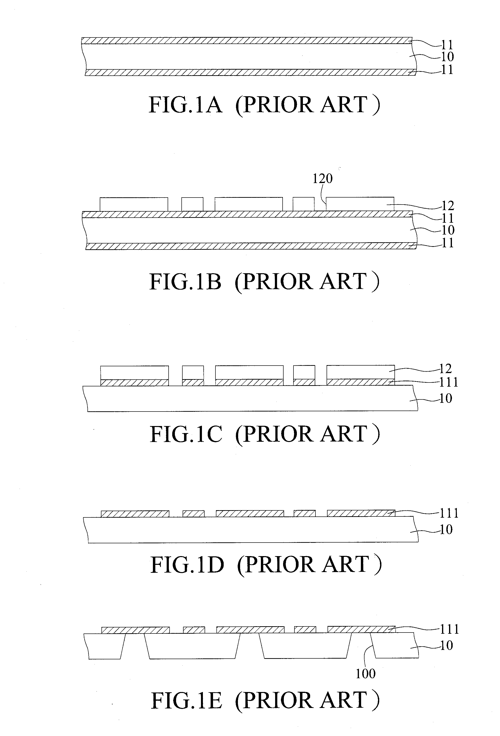
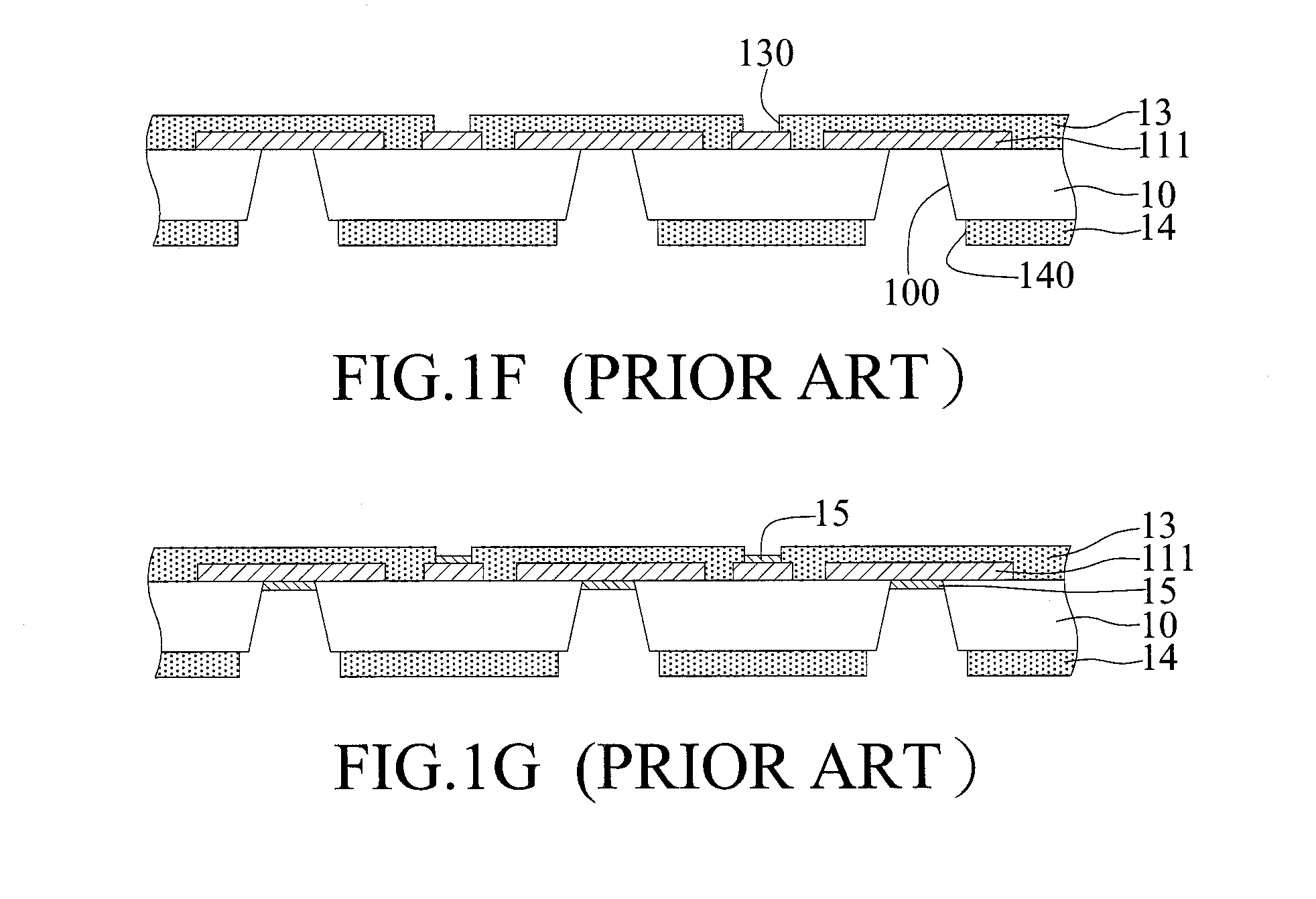
However, the packaging substrate still has the carrier board unremoved that supports the circuit layer.
The overall packaging substrate is about 130 μm thick, and is approximately as thick as a general packaging substrate having two layer circuits, which is adverse to the compact-sized and low-profiled requirements.
Hence, how to provide a thinner packaging substrate is becoming one of the most popular issues in the art.

Method used


Image

  • Packaging substrate and method of fabricating the same
  • Packaging substrate and method of fabricating the same
  • Packaging substrate and method of fabricating the same

Examples


first embodiment

[0041]Please refer to FIGS. 2A through 2I, which are cross-sectional views illustrating a method of fabricating a packaging substrate of a first embodiment according to the present invention, wherein FIG. 2G′ and 2G″ are top views depicting different embodiments of FIG. 2G, and FIGS. 2H′ and 2I′ are another embodiments of FIGS. 2H and 2I, respectively.

[0042]As shown in FIG. 2A, a metal board 20 is provided that has a first surface 20a and an opposing second surface 20b.

[0043]As shown in FIG. 2B, a resist layer 21 is formed on the first surface 20a, the resist layer 21 having a plurality of patterned open areas 210 exposing the first surface 20a.

[0044]As shown in FIG. 2C, a portion of the metal board 20 that is uncovered by the resist layer 21 is removed, to form a sunken area 200 and a plurality of metal raised portions 201 preparing to serve as a circuit layer.

[0045]As shown in FIG. 2D, the resist layer 21 is removed. The circuit layer, namely the metal raised portions 201, compr...

second embodiment

[0057]Please refer to FIGS. 3A through 3D, which are cross-sectional views illustrating a method of fabricating a packaging substrate of a second embodiment according to the present invention, wherein FIG. 3D′ is another embodiment of FIG. 3D.

[0058]As shown in FIG. 3A, which is derived from FIG. 2D, a dielectric layer 22 is formed on the first surface 20a and the sunken area 200. In an embodiment of the present invention, the dielectric layer 22 is made of epoxy.

[0059]As shown in FIG. 3B, a plurality of conductive pad openings 220 are formed in the dielectric layer 22 to expose the conductive pads 201b. In an embodiment of the present invention, the conductive pad openings 220 may be formed by laser ablation or photolithography processes.

[0060]As shown in FIG. 3C, a partial thickness of the metal board 20 is removed to expose the metal raised portions 201.

[0061]As shown in FIG. 3D, an insulating protective layer 29 is formed on the second surface 20b to cover the metal raised portio...

third embodiment

[0063]Please refer to FIGS. 4A through 4D, which are cross-sectional views illustrating a method of fabricating a packaging substrate of a third embodiment according to the present invention, wherein FIG. 4D′ is another embodiment of FIG. 4D.

[0064]The third embodiment is different from the second embodiment in that the dielectric layer 22 is made of solder-resist material in the third embodiment, while epoxy in the second embodiment.

[0065]The present invention further discloses another packaging substrate, comprising: a dielectric layer 22 having an external contact surface 22a and an opposing chip mounting surface 22b; and a circuit layer embedded in the dielectric layer 22 and having wire-bonding pads 201a, conductive pads 201b, and circuit 201c that electrically connects the wire-bonding pads 201a and the conductive pads 201b. The circuit layer is exposed from the chip mounting surface 22b, and the external contact surface 22a of the dielectric layer 22 has a plurality of conduct...


PUM

PropertyMeasurementUnit
thickaaaaaaaaaa
dielectricaaaaaaaaaa
thicknessaaaaaaaaaa

Abstract

A packaging substrate and a method of fabricating the packaging substrate. The packaging substrate includes: a dielectric layer that has an external contact surface and an opposing chip mounting surface; a circuit layer that is embedded in the dielectric layer and exposed from the external contact surface and the chip mounting surface, the circuit layer having wire-bonding pads, conductive pads, and a circuit that electrically connects the wire-bonding pads and the conductive pads, wherein the widths of the wire-bonding pads, conductive pads, and the circuit narrow gradually from chip mounting surface to the external contact surface; and a first insulating protective layer disposed on the external contact surface of the dielectric layer and covering the dielectric layer and the circuit layer, a plurality of conductive pad openings being formed in the first insulating protective layer for exposing the conductive pads. The dielectric layer is used directly as a foundation of the packaging substrate, thereby providing advantage in miniaturization, simpler fabrication procedure, and thus low cost production.

Description

BACKGROUND OF THE INVENTION[0001]1. Field of the Invention[0002]This invention relates to a packaging substrates and methods of fabricating the same, and, more particularly, to a packaging substrate having a single circuit layer, and a method of fabricating the packaging substrate.[0003]2. Description of Related Art[0004]A lead frame packaging substrate has been long used in a semiconductor chip package, since it has a low cost and high reliability. For a semiconductor chip having a small number of I / Os, the lead frame packaging substrate is still competitive in the cost.[0005]A simple electronic product may need a packaging substrate having a single layer circuit.[0006]Please refer to FIGS. 1A through 1G, which are cross sectional views illustrating a method of fabricating a packaging substrate having a single circuit layer according to the prior art.[0007]As shown in FIG. 1A, a carrier board 10 is provided that has copper layers 11 disposed on both sides thereof.[0008]As shown in ...

Claims


Application Information

Patent Timeline
Patent Type & Authority Applications(United States)
IPC IPC(8): H05K1/02H05K3/10
CPCH01L23/3121H01L23/49827H01L23/49861H01L24/48H01L2224/48091H01L2224/32225H01L2224/73265H01L2224/85444Y10T29/49155H01L2224/48227H01L2224/48235H01L2924/00014H01L2924/00012H01L24/73H01L2924/181H01L2224/45099H01L2224/45015H01L2924/207
Inventor CHOU, PAO-HUNGCHANG, HSIEN-MIN
Owner UNIMICRON TECH CORP
Learn More