
Template Process for Small Pitch Flip-Flop Interconnect Hybridization

a flip-chip interconnect and template technology, applied in the field of template process for small pitch flip-chip interconnect hybridization, can solve the problems of increasing the difficulty of hybridizing two chips with a high yield of successful bonds, other components are not monolithically fabricated on the same chip, and the pitch of flip-chip interconnects has gotten smaller. , to achieve the effect of eliminating non-uniform bump shape and siz

Inactive Publication Date: 2011-04-07
UNITED STATES OF AMERICA THE AS REPRESENTED BY THE SEC OF THE ARMY
View PDF9 Cites 5 Cited by
  • Summary
  • Abstract
  • Description
  • Claims
  • Application Information

AI Technical Summary

Benefits of technology

"The patent describes a process for making high-density indium bumps on microchips using a reusable template wafer. This process involves fabricating bumps on the template wafer and then transferring them to the microchip. The template wafer is reusable and helps to ensure uniform bump shape and size between separate microchips. The process is economical and efficient, and it allows for the fabrication of tall indium bumps with a high aspect ratio. This is important for ensuring proper compliance with strain caused by differences in the thermal coefficient of expansion of the two microchips when they are hybridized."

Problems solved by technology

In many cases, these other components are not monolithically fabricated on the same chip, where they could be easily interconnected through a variety of techniques.
Like most things in the microelectronics industry, the pitch of these flip-chip interconnects has gotten smaller over time.
This small pitch makes it increasingly difficult to hybridize two chips with a high yield of successful bonds.
However, for a variety of reasons, these techniques are generally not suitable when bonding together chips that are composed of different substrate materials.
As this pitch falls below 10 μm, current technology will become less capable of successfully hybridizing the two microchips.
The fabrication process described provides a way to form relatively tall indium bumps and accomplishes this without the standard thick photoresist liftoff process, which makes it nearly impossible to fabricate relatively tall bumps with a pitch under 10 microns.
The described process is suitable for bump pitches under 10 microns and is only limited by the resolution of the photolithography equipment used.

Method used


Image

  • Template Process for Small Pitch Flip-Flop Interconnect Hybridization
  • Template Process for Small Pitch Flip-Flop Interconnect Hybridization
  • Template Process for Small Pitch Flip-Flop Interconnect Hybridization

Examples


second exemplary embodiment

Alternate Teflon™ Deposition Techniques

[0045]Another exemplary embodiment follows FIGS. 2a-e. The following steps occur in the same manner as the initial exemplary embodiment: degreasing and oxide etching dip of the Si wafer, about 500 nanometer to 1 micron topside Ni deposition and 200 nanometer Al deposition, and backside about 500 nanometer to 1 micron Ni deposition and 200 nanometer Al deposition. This exemplary embodiment uses a different set of techniques to deposit the topside nonconductive layer 207 and backside nonconductive layer 208 of FIG. 2b. Instead of using spin-on Teflon™ AF 1601-S to deposit these layers, PTFE can be deposited in a vacuum chamber onto the conductive layer of the transfer wafer 206 shown in FIG. 2a. One can use either RF sputtering deposition or atomic layer deposition (ALD) to perform deposition of PTFE. The thickness of the deposition of the topside nonconductive layer can be chosen to be roughly 1 to 2 microns less than the desired final height of...

third exemplary embodiment

Etching Notches

[0047]Yet another exemplary embodiment follows FIG. 2a. The following steps occur in the same manner as the initial exemplary embodiment: degreasing and oxide etching dip of the Si wafer, about 500 nanometer to 1 micron topside Ni deposition and 200 nanometer Al deposition, backside about 500 nanometer to 1 micron Ni deposition and 200 nanometer Al deposition, deposition of the topside nonconductive layer by either of the techniques described in the previous exemplary embodiments, and deposition of the backside nonconductive layer by either of the techniques described in the previous exemplary embodiments.

[0048]FIG. 3a shows how fabrication proceeds for this exemplary embodiment. Just as in the initial exemplary embodiment, a 200 nanometer Al etch mask 303 is deposited on the nonconductive layer 301 by the same techniques. After the Al deposition, a standard photolithography step is performed to define features in the photoresist layer 304. These features, unlike the ...

fourth exemplary embodiment

Imprint Fabrication

[0052]Yet, another exemplary embodiment follows FIG. 2a. The following steps occur in the same manner as the initial embodiment: degreasing and oxide etching dip of the Si wafer, about 500 nanometer to 1 micron topside Ni deposition and 200 nanometer Al deposition, backside about 500 nanometer to 1 micron Ni deposition and 200 nanometer Al deposition, deposition of the topside nonconductive layer by either of the techniques described in the previous embodiments, and deposition of the backside nonconductive layer by either of the techniques described in the previous embodiments.

[0053]This exemplary embodiment differs from previous ones in the way that the features on the topside nonconductive layer are defined. Rather than using an etch mask followed by etching, this exemplary embodiment involves imprinting the topside nonconductive layer with features defined on another wafer, to be called the imprinting wafer. The result is that the features on the nonconductive ...


PUM


Abstract

A process is disclosed for high density indium bumping of microchips by using an innovative template wafer upon which the bumps are initially fabricated. Once fabricated, these bumps are transferred to the microchip, after which can be hybridized to another microchip. Such a template wafer is reusable, and thus provides an economical way to fabricate indium bumps. Reusability also eliminates nonuniformities in bump shape and size in serial processing of separate microchips, which is not the case for other indium bump fabrication processes. Such a fabrication process provides a way to form relatively tall indium bumps and accomplishes this without the standard thick photoresist liftoff process. The described process can be suitable for bump pitches under 10 microns, and is only limited by the resolution of the photolithography equipment used.

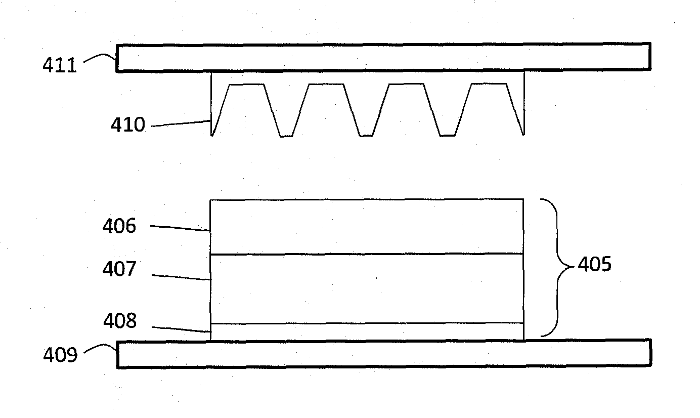
Description

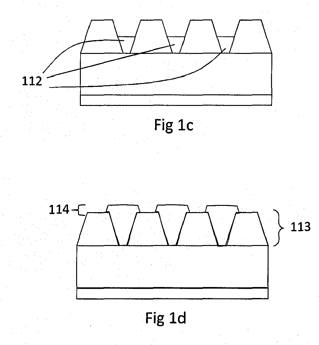
GOVERNMENT INTEREST[0001]The invention described herein may be manufactured, used, sold, imported and / or licensed by or for the United States Government.FIELD OF THE DISCLOSURE[0002]The disclosure relates to a process for fabricating high density indium bumps based on a template wafer, and transfer of these bumps to hybridize microchips.BACKGROUND INFORMATION[0003]Devices that contain microelectronic components generally require a transfer of information from the chip to one or several other components on the system. In many cases, these other components are not monolithically fabricated on the same chip, where they could be easily interconnected through a variety of techniques. Instead, a highly conductive layer sandwiched between two components is required to transfer information. One of the industry standard ways to do this it by flip-chip bump bonding. This technique requires the deposition of a soft conductive material to be deposited on either one or both of the microchips to ...

Claims


Application Information

Patent Timeline
Patent Type & Authority Applications(United States)
IPC IPC(8): H01L23/48H01L21/60
CPCH01L24/11H01L21/76885H01L2924/01013H01L2924/01015H01L2924/01018H01L2924/01027H01L2924/01049H01L2924/01078H01L2924/14H01L24/13H01L24/16H01L24/742H01L2224/11003H01L2224/11334H01L2224/16148H01L2224/742H01L2224/81203H01L2924/00013H01L2924/01006H01L2924/01019H01L2924/01033H01L2924/01072H01L2224/111H01L2224/13109H01L2924/01204H01L2224/13099H01L2224/05099H01L2224/13599H01L2224/05599H01L2224/29099H01L2224/29599
Inventor MARKUNAS, JUSTIN K.SCHULTE, ERIC F.
Owner UNITED STATES OF AMERICA THE AS REPRESENTED BY THE SEC OF THE ARMY
Learn More