
METHOD FOR Sr-Ti-O-BASED FILM FORMATION AND STORAGE MEDIUM

Inactive Publication Date: 2011-01-20
TOKYO ELECTRON LTD +1
View PDF4 Cites 2 Cited by
  • Summary
  • Abstract
  • Description
  • Claims
  • Application Information

AI Technical Summary

Benefits of technology

[0007]The object of the present invention is to provide a method for forming a Sr—Ti—O-based film, which can stably generate a SrTiO3 crystal.
[0008]It is another object of the present invention to provide a method for forming a Sr—Ti—O-based film, in which a required ratio of Sr and Ti can be achieved.
[0009]It is a further object of the present invention to provide a method for forming a Sr—Ti—O-based film, in which an oxidant can rapidly reach a supply saturation point and required SrO is formed, thereby obtaining a satisfactory Sr—Ti—O-based film.
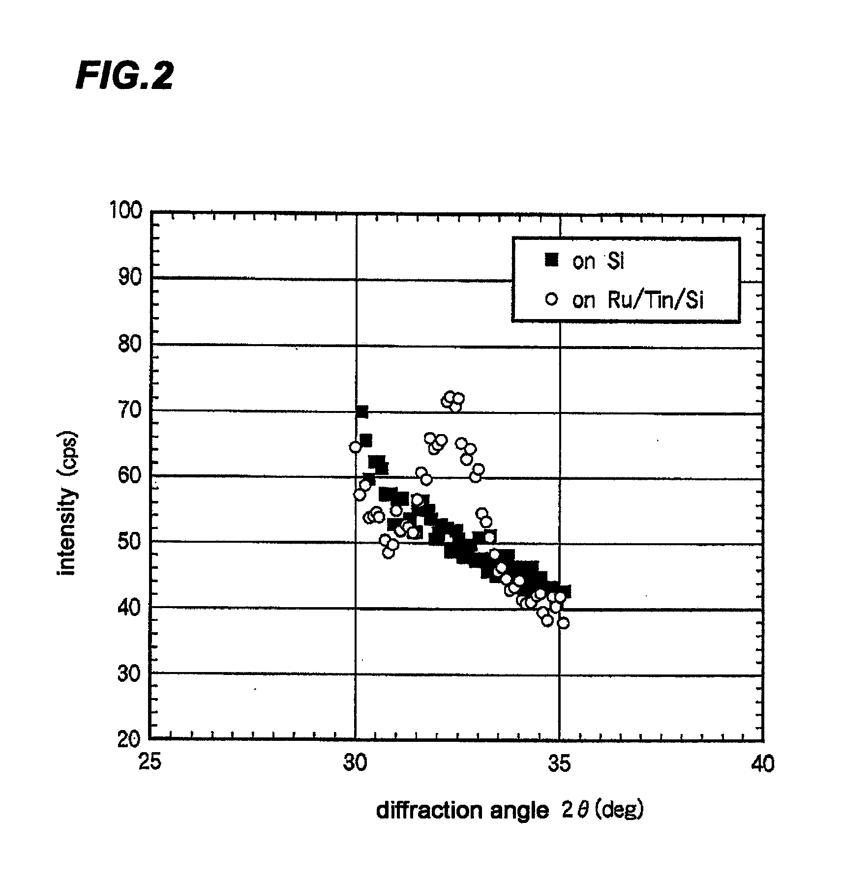
[0020]According to the present invention, since the film formation is carried out in such a manner that a Sr / Ti ratio within a film can be in a range of 1.2 to 3 in a ratio of the number of atoms, and the formed film is annealed in atmosphere containing O2 of 0.001% to 80% at 500° C. or more, it is possible to stably generate an SrTiO3 crystal in a thin film of 7 to 20 nm. In other words, after the film formation with a certain composition with a large amount of Sr, the crystallization of SrTiO3 is achieved by the migration of Ti to the surface through annealing under the existence of O2. Thus, it is possible to achieve the crystallization in the thin film.
[0021]Also, according to the present invention, a sequence for continuously performing only one or both of a SrO film formation process and a TiO film formation process multiple times is repeated multiple times. Accordingly, even in a condition where adsorption inhibition may be caused according to the combination of raw materials, such adsorption inhibition can be avoided while the same film formation process is continuously repeated. Thus, it is possible to obtain a Sr—Ti—O-based film with the required composition.

Problems solved by technology

However, in forming a thin film by such a method, it is difficult to crystallize the thin film even with a stoichiometric composition of Sr:Ti=1:1 through annealing following the film formation depending on the kind of a substrate.
However, in this method, adsorption may be inhibited according to the combination of raw materials.
However, when O3 is used as an oxidant, it takes a longer time to reach the saturation point depending on the kind of an organic Sr compound used as a Sr raw material, and the film thickness becomes very thick (0.3 to 0.4 nm) per 1 cycle at the saturation point.

Method used


Image

  • METHOD FOR Sr-Ti-O-BASED FILM FORMATION AND STORAGE MEDIUM
  • METHOD FOR Sr-Ti-O-BASED FILM FORMATION AND STORAGE MEDIUM
  • METHOD FOR Sr-Ti-O-BASED FILM FORMATION AND STORAGE MEDIUM

Examples


first exemplary embodiment

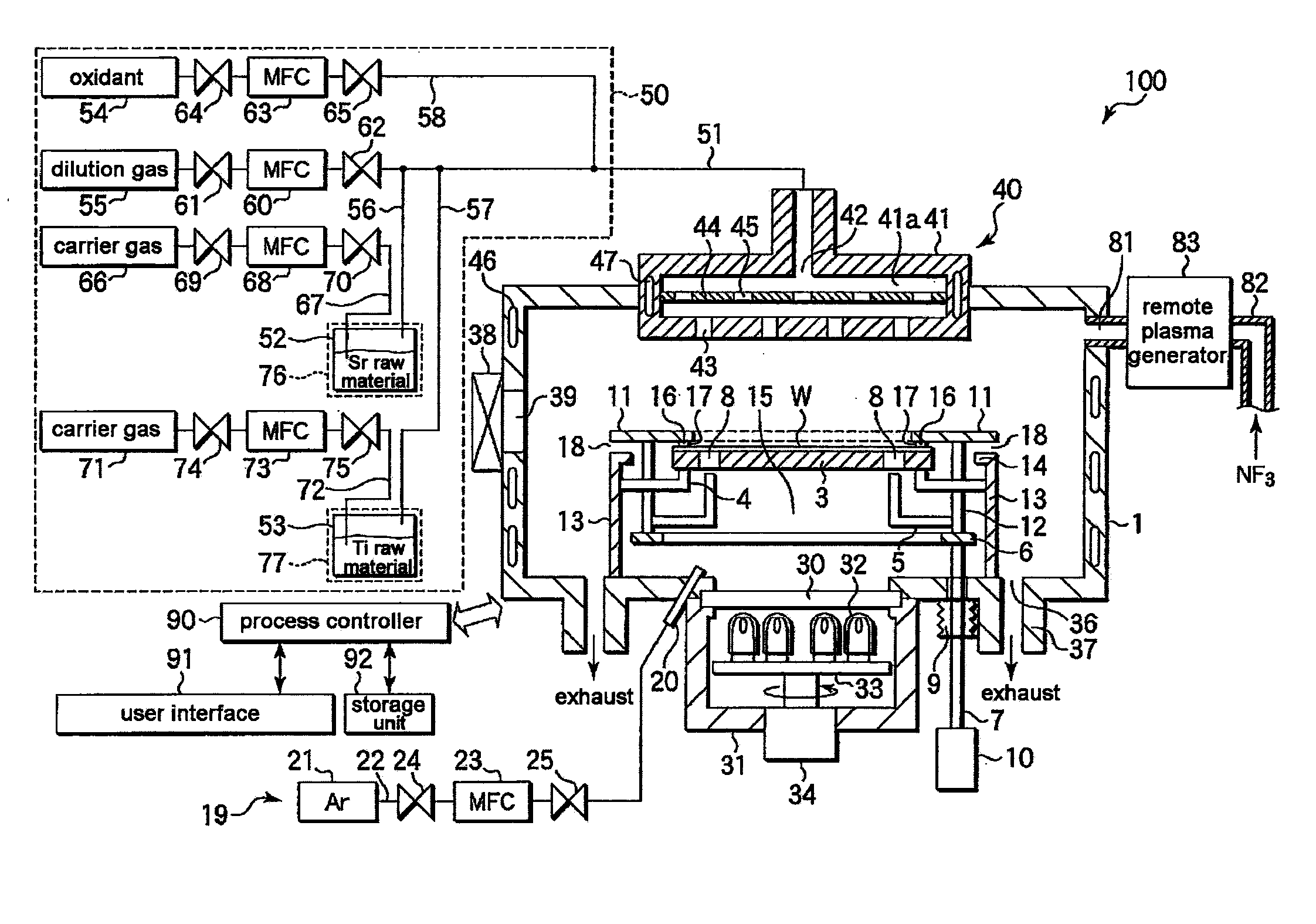
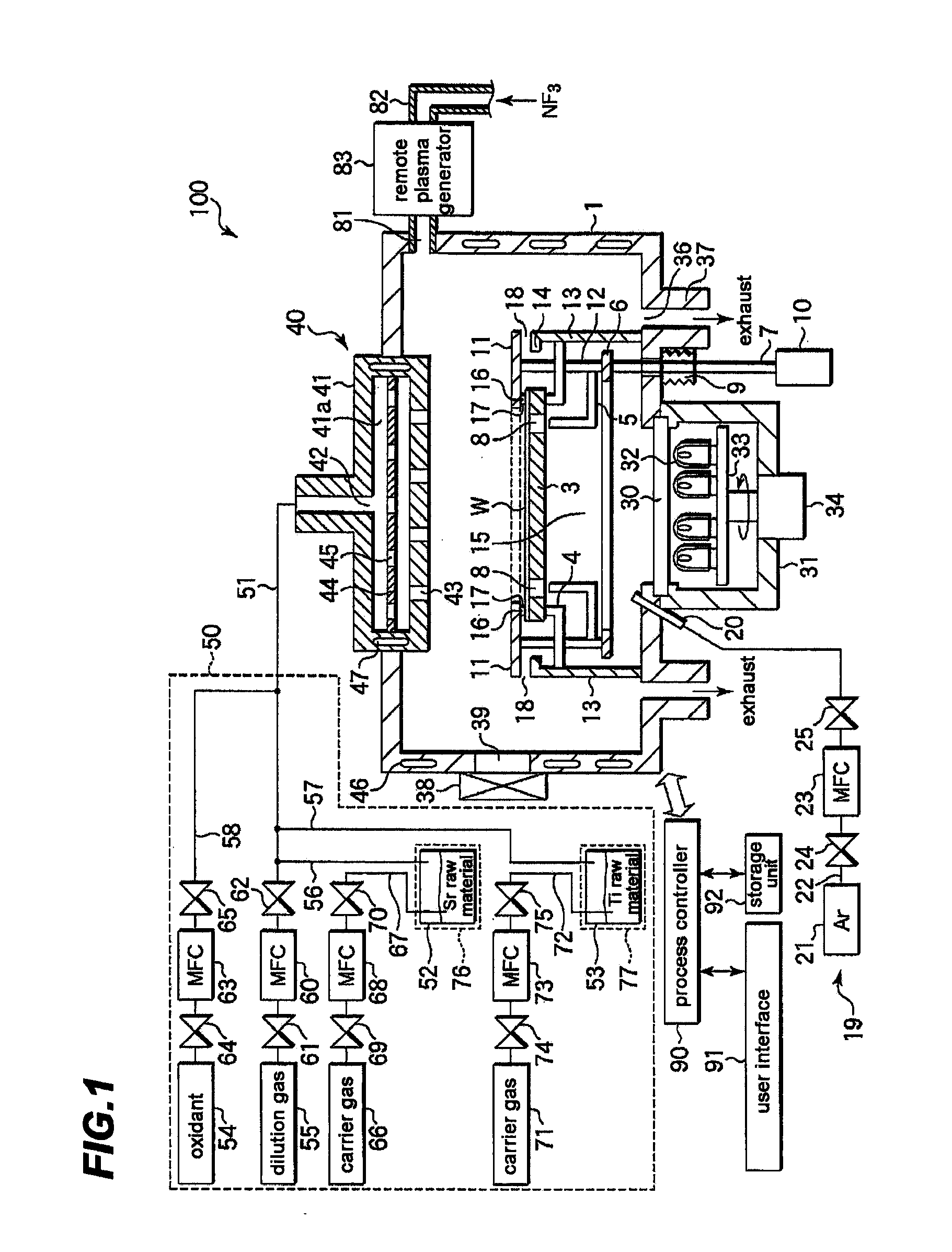
[0055]In the first exemplary embodiment, at first, gate valve 38 is opened and a semiconductor wafer W is taken into processing chamber 1 through loading / unloading hole 39 and is loaded on loading table 3. Loading table 3 has been heated by heat rays which were previously emitted from heating lamps 32 and transmitted from transmission window 30. Semiconductor wafer W is heated by the heat of loading table 3. Then, dilution gas source 55 supplies dilution gas, such as Ar gas, at a flow rate of 100 to 800 mL / sec(sccm). Meanwhile, the inside of processing chamber 1 is exhausted by a vacuum pump (not shown) via exhaust hole 36 and exhaust pipe 37, thereby forming a pressure of approximately 39 to 665 Pa within processing chamber 1. Herein, the heating temperature of semiconductor wafer W is set to be within a range of 200 to 400° C.

[0056]Then, the film formation is actually started by controlling the flow rate of the dilution gas, such as Ar gas, to be in a range of 100 to 500 mL / sec(sc...

second exemplary embodiment

[0085]In the same manner as the first exemplary embodiment, in the second exemplary embodiment, gate valve 38 is opened first, and a semiconductor wafer W is taken from loading / unloading hole 39 into processing chamber 1 and is loaded on loading table 3. Since loading table 3 has been previously heated by heating lamps 32, semiconductor wafer W is heated up to a predetermined temperature, for example, 200 to 400° C. Then, dilution gas, such as Ar gas, is supplied from dilution gas source 55 at a flow rate of 100 to 800 mL / sec (sccm). Meanwhile, the inside of processing chamber 1 is exhausted by a vacuum pump (not shown) via exhaust hole 36 and exhaust pipe 37, thereby vacuum-exhausting processing chamber 1 so that the pressure within processing chamber 1 is approximately 6 to 665 Pa. Then, the film formation is actually started by controlling the flow rate of the dilution gas, such as Ar gas, to be in a range of 100 to 500 mL / sec (sccm) and controlling the pressure within processing...

third exemplary embodiment

[0104]In the same manner as the first exemplary embodiment, in the third exemplary embodiment, gate valve 38 is opened first, and a semiconductor wafer W is taken from loading / unloading hole 39 into processing chamber 1 and is loaded on loading table 3. Since loading table 3 has been previously heated by heating lamps 32, semiconductor wafer W is heated up to a predetermined temperature, for example, 200 to 400° C. Then, dilution gas, such as Ar gas, from dilution gas source 55 is supplied at a flow rate of 100 to 800 mL / sec (sccm). Meanwhile, the inside of processing chamber 1 is exhausted by a vacuum pump (not shown) via exhaust hole 36 and exhaust pipe 37, thereby vacuum-exhausting processing chamber 1 so that the pressure within processing chamber 1 is approximately 39 to 665 Pa. Then, the film formation is actually started by controlling the flow rate of the dilution gas, such as Ar gas, to be in a range of 100 to 500 mL / sec (sccm) and controlling the pressure within processing...


PUM

PropertyMeasurementUnit
Fractionaaaaaaaaaa
Fractionaaaaaaaaaa
Ratioaaaaaaaaaa

Abstract

A film is formed so that the atomic numbers ratio of Sr to Ti, i.e., Sr / Ti, in the film is not less than 1.2 and not more than 3. The film is then annealed in an atmosphere containing not less than 0.001% and not more than 80% of O2 at 500° C. or above. An SrO film forming step or a TiO film forming step are repeated a plurality of times so that a sequence, in which a plurality of SrO film forming steps or / and a plurality of TiO film forming steps are performed continuously, is included. When Sr is oxidized after the adsorption of Sr, O3 and H2O are used as an oxidizing agent.

Description

TECHNICAL FIELD[0001]The present invention relates to a method to form a Sr—Ti—O-based film, such as a SrTiO3 film, and a storage medium.BACKGROUND[0002]In the semiconductor device, an integrated circuit has become highly integrated, and a DRAM has required the reduction of size and the enlargement of memory capacity of a memory cell. For this requirement, an MIM (metal-insulator-metal) structure capacitor has been spotlighted. Such a MIM structure capacitor uses a high dielectric material, such as strontium titanate (SrTiO3), as an insulating film (dielectric film).[0003]In the formation of a SrTiO3 film for a DRAM capacitor, a method for forming a film by ALD has been conventionally widely used, in which an organic Sr raw material and an organic Ti raw material are used, and O3 gas is used as an oxidant, [for example, “Plasma enhanced atomic layer deposition of SrTiO3 thin films with Sr(tmhd)2 and Ti(i-OPr)4” J. Vac. Scl. Technol. A20(5), J. H. Lee et al. September / October 2002].[...

Claims


Application Information

Patent Timeline
IPC IPC(8): H01L21/30
CPCC23C16/409C23C16/45531H01L21/31691H01L21/67115H01L21/31604H01L28/55H01L21/02197H01L21/0228H01L21/68742H01L21/02186H01L21/02263H01L21/02356H01L21/02337
Inventor KAWANO, YUMIKOARIMA, SUSUMUKAKIMOTO, AKINOBUHIROTA, TOSHIYUKIKIYOMURA, TAKAKAZU
Owner TOKYO ELECTRON LTD
Learn More