Trench mosfet with shallow trench contact

Inactive Publication Date: 2010-04-15
FORCE MOS TECH CO LTD
View PDF9 Cites 29 Cited by
  • Summary
  • Abstract
  • Description
  • Claims
  • Application Information

AI Technical Summary

Benefits of technology

[0007]It is therefore an object of the present invention to provide new and improved trench MOSFET element and manufacture process to prevent the P+ area touching to channel region issue and gate / drain shortage issue from happening, and to make a better connection performance while maintaining a lower cost.
[0008]One aspect of the present invention is that, a shallow trench contact structure is invented to resolve some of the problems discussed above. First, while employing this shallow trench contact structure, contact silicon depth (Dcsi) is shallower than n+ source depth (Dn+), which well avoids the P+ area touching to channel region issue due to n+ source blocking P+ area from lateral diffusion as stopper, thus, the relevant increasing of Rds can be prevented. FIG. 3 shows that when a wider contact CD is applied, P+ around the source-body contact trench bottom is inherently blocked by n+ source, which makes more contact CD tolerance. On the other hand, since the contact trench is shallower than conventional, Al alloys can refill the trench contact with good metal step coverage instead of W metal plug in some preferred embodiments, making a cost down for mass production. However, different from the traditional process, in order to implement this shallow trench contact structure, after the P-body area formation, Ion Implantation is applied first to form n+ source layer, then contact trenches are etch through thick contact oxide layer and n+ source layer, and n+ source diffusion is subsequently followed to form a given n+ source depth which is deeper than source contact trench.
[0009]Another aspect of the present invention is that, the MOSFET further includes trench floating rings as termination to avoid degradation of breakdown voltage resulted from shallow trench structure.
[0010]Another aspect of the present invention is that, the bottom of all trench gates, including floating trench gates, are wrapped with n* areas which are heavier doped than epitaxial layer to further reduce Rds.
[0011]Another aspect of the present invention is that, terrace gate structure is applied in some preferred embodiments to avoid the gate contact trench etching through gate oxide issue. Meanwhile, the terrace gate structure can further reduce Rg as terrace trench gate provides additional poly over silicon mesa area; At the same time, a self-aligned source contact is achieved by this terrace gate structure solving avalanche current and Rds non-uniform distribution issue resulted from misalignment between trench contact and trench gate.

Problems solved by technology

On the other hand, since the contact trench is shallower than conventional, Al alloys can refill the trench contact with good metal step coverage instead of W metal plug in some preferred embodiments, making a cost down for mass production.

Method used


Image

  • Trench mosfet with shallow trench contact
  • Trench mosfet with shallow trench contact
  • Trench mosfet with shallow trench contact

Examples


first embodiment

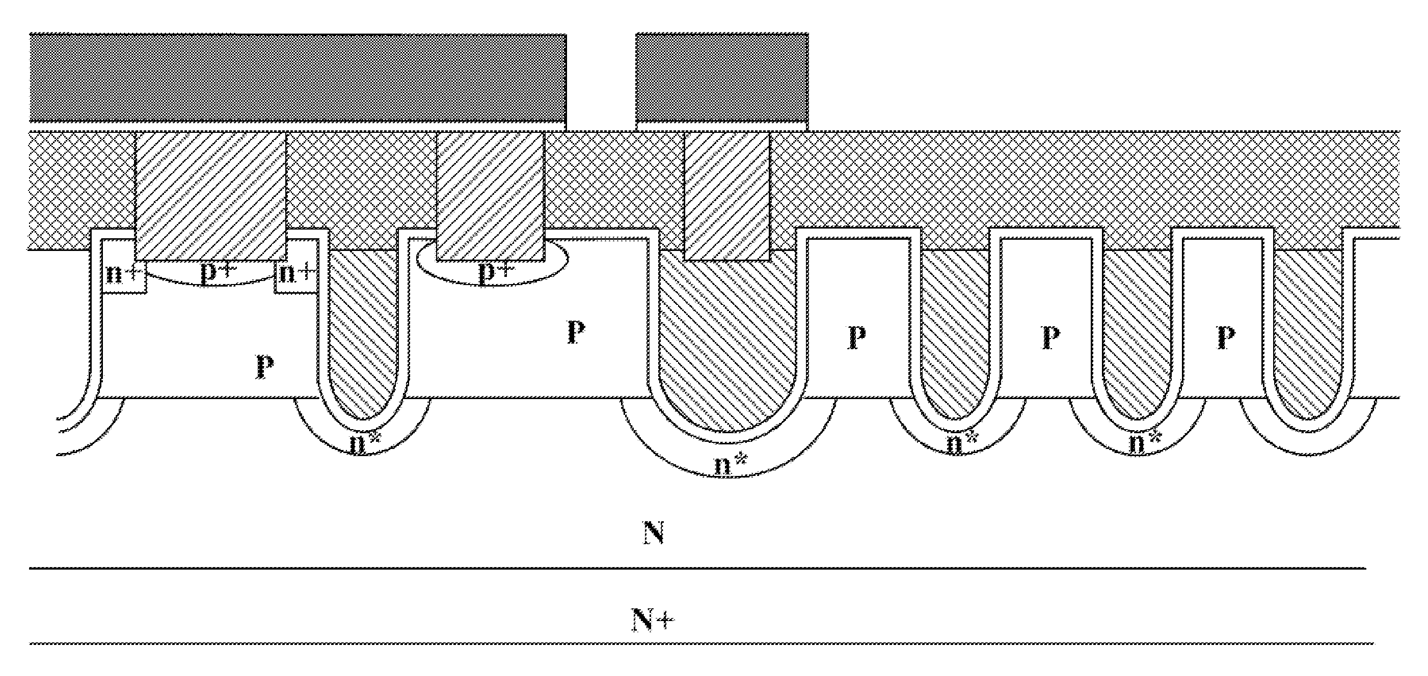
[0036]Please refer to FIG. 5 for a second preferred embodiment of this invention, wherein the trench MOSFET has the same structure with the first embodiment, except that the material used as contact trench filler and front metal are both Al alloys. That's because Al alloys can refill the shallower trench contact with good metal step coverage, thus making a lower cost than using of tungsten plug.

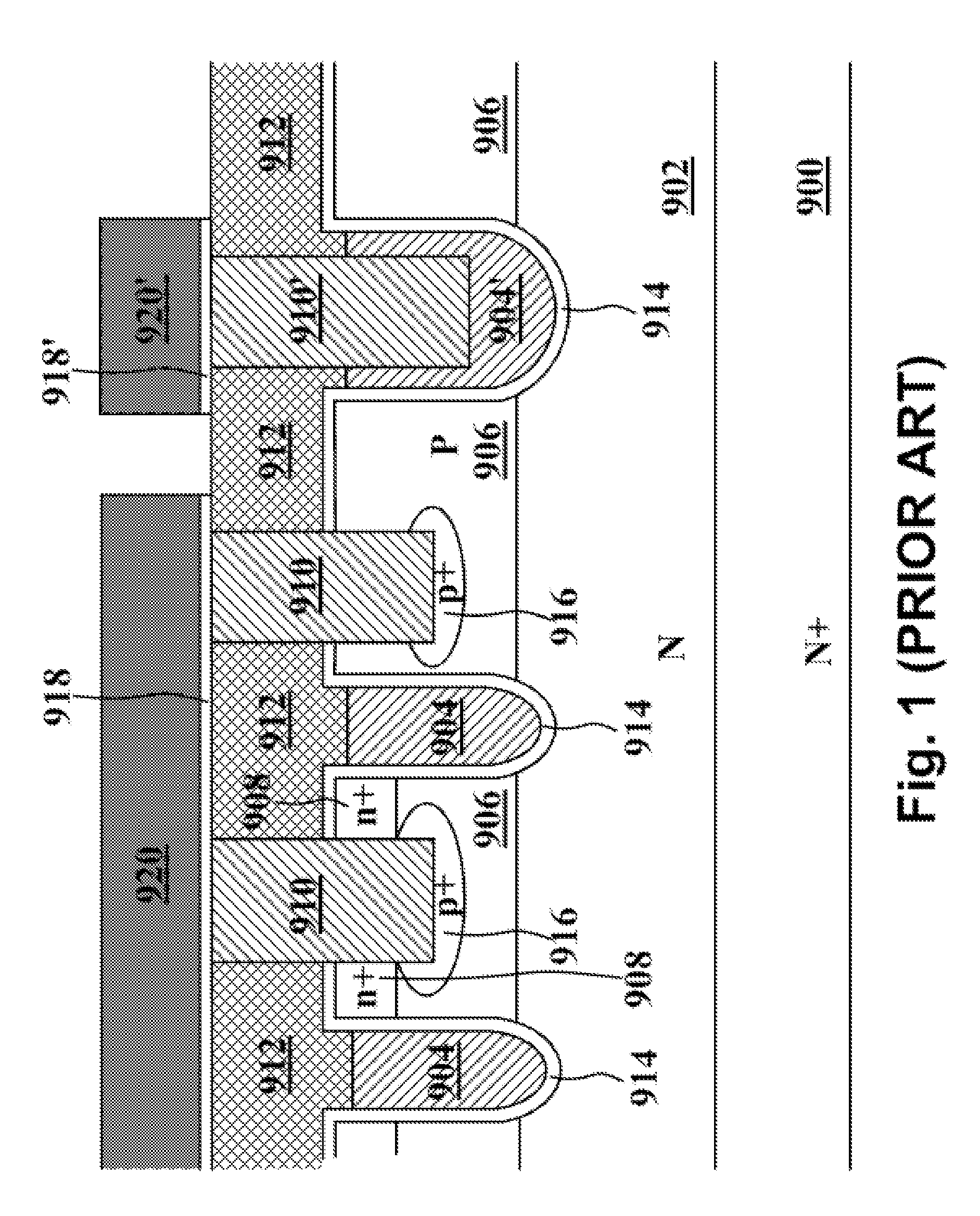
[0037]For the purpose of avoiding the trench gate contact penetrating through doped poly and gate oxide layer and resulting in shortage of metal plug to epitaxial layer when the gate trenches becomes shallower, a terrace poly gate is employed in a third preferred embodiment, as shown in FIG. 6. The trench MOSFET of this embodiment is formed on an N+ substrate 140 coated with back metal Ti / Ni / Ag 141 on rear side as drain. Onto said substrate 40, grown an N epitaxial layer 142, and a plurality of trenches 124a (not shown), 124′a (not shown) and 125a (not shown) were etched wherein, especially, ...

third embodiment

[0038]Please refer to FIG. 7 for a fourth preferred embodiment of this invention, wherein the trench MOSFET has the same structure with the third embodiment, except that the material used as trench contact filler and front metal are both Al alloys. That's because Al alloys can refill the shallower trench contact with good metal step coverage, thus making a lower cost than using of tungsten plug.

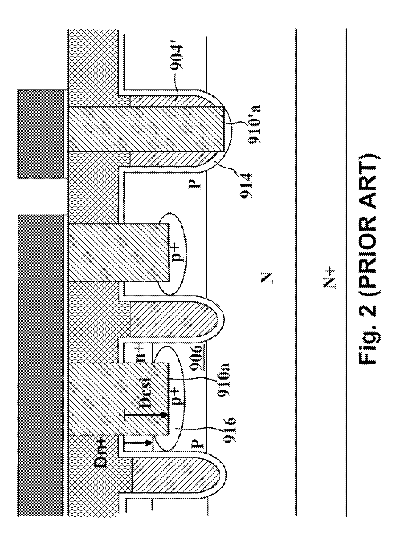
[0039]Please refer to FIG. 8 for a fifth preferred embodiment of this invention, wherein the trench MOSFET has the same structure with the first embodiment, except that there is an additional P* region 136 underneath each P+ area around the bottom of trench source-body contact. The P* region is Ion Implanted with dose less than P+ area but higher than P-body for avalanche energy improvement without significantly affecting threshold voltage due to lighter dose than P+ area. At the same time, the P* area Ion Implantation energy is higher than P+ region to form P* underneath P+.

second embodiment

[0040]Please refer to FIG. 9 for a sixth preferred embodiment of this invention, wherein the trench MOSFET has the same structure with the second embodiment, except that there is additional P* region 136 underneath each P+ area around the bottom of trench source-body contact. The P* region is Ion Implanted with dose less than P+ area but higher than P-body for avalanche energy improvement without significantly affecting threshold voltage due to lighter dose than P+ area. At the same time, the P* area Ion Implantation energy is higher than P+ region to form P* underneath P+.

[0041]Please refer to FIG. 10 for a seventh preferred embodiment of this invention, wherein the trench MOSFET has the same structure with the third embodiment, except that there is additional P* region 136 underneath each P+ area around the bottom of trench source-body contact. The P* region is Ion Implanted with dose less than P+ area but higher than P-body for avalanche energy improvement without significantly a...


PUM


Abstract

A trench MOSFET element with shallow trench contact is disclosed. This shallow trench contact structure has some advantages: blocking the P+ underneath trench contact from lateral diffusion to not touch to channel region when a larger trench contact CD is applied; avoiding the trench gate contact etching through poly and gate oxide when trench gate becomes shallow; making lower cost to refill the trench contact using Al alloys with good metal step coverage as the trench contact is shallower. The disclosed trench MOSFET element further includes an n* region around the bottom of gate trenches to reduce Rds. In some embodiment, the disclosed trench MOSFET provides a terrace gate to further reduce Rg and make self-aligned source contact; In some embodiment, the disclosed trench MOSFET comprises a P* area underneath said P+ region for avalanche energy improvement with lighter dose than said P+ region.

Description

FIELD OF THE INVENTION[0001]This invention relates generally to the cell configuration and fabrication process of trench MOSFET devices. More particularly, this invention relates to a novel and improved cell structure and improved process of fabricating a trench MOSFET with shallow trench contact.BACKGROUND[0002]A trench MOSFET with conventional deep trench contact is disclosed in FIG. 1. This trench MOSFET of prior art further comprises: a heavily N+ doped substrate 900; an N epitaxial layer 902 with lighter concentration than said substrate 900; a plurality of narrower gate trenches 904a (not shown) and at least a wider gate trench 904′a (not shown) for gate contact are etched into said epitaxial layer 902, said narrower gate trenches 904a and at least a wider gate trench 904′a are filled with doped poly to serve as narrower trench gates 904 and at least a wider trench gate 904′ for gate contact over a gate oxide layer 914; a plurality of P-body regions 906 formed in said epitaxia...

Claims


Application Information

Patent Timeline
IPC IPC(8): H01L29/78H01L21/336
CPCH01L29/0878H01L29/1095H01L29/407H01L29/41766H01L29/4236H01L29/7813H01L29/456H01L29/66727H01L29/66734H01L29/7811H01L29/42372
Inventor HSIEH, FU-YUAN
Owner FORCE MOS TECH CO LTD
Why Eureka
Try Eureka