
Nanowire and microwire fabrication technique and product

a technology of nanowires and microwires, applied in the field of nanotechnology, can solve the problems of difficult fabrication of nanowire devices, irregular orientation of nanowires, and difficulty in controlling the geometry of step edges on the hopg substrate, and achieve the effect of low cohesion

Active Publication Date: 2009-10-01
WISYS TECH FOUND
View PDF3 Cites 25 Cited by
  • Summary
  • Abstract
  • Description
  • Claims
  • Application Information

AI Technical Summary

Benefits of technology

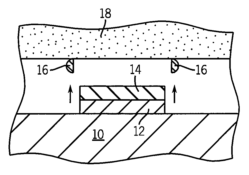
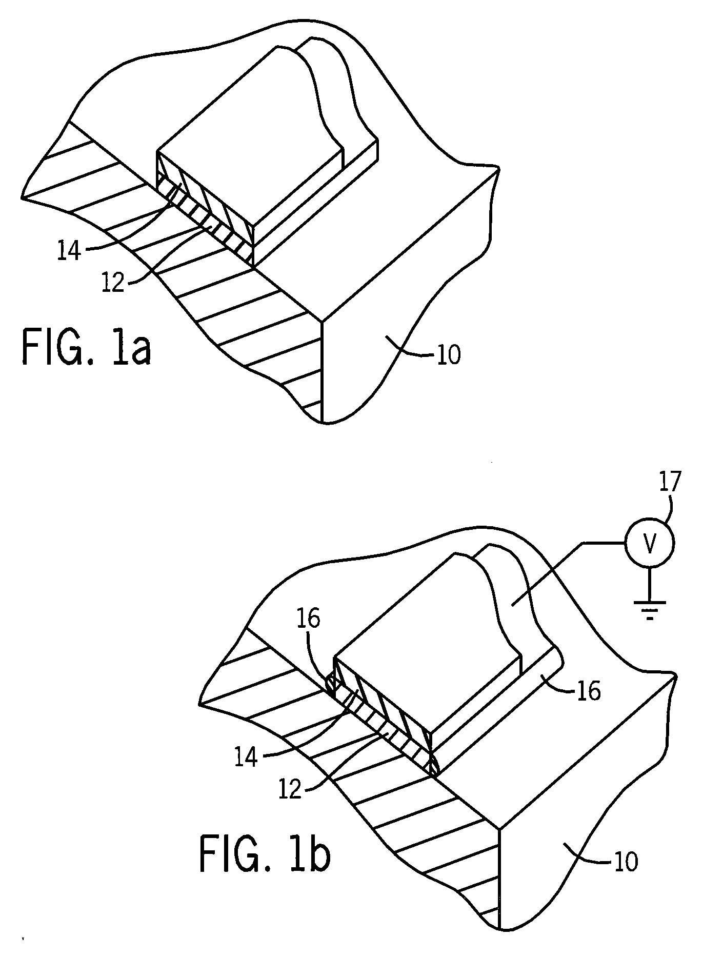
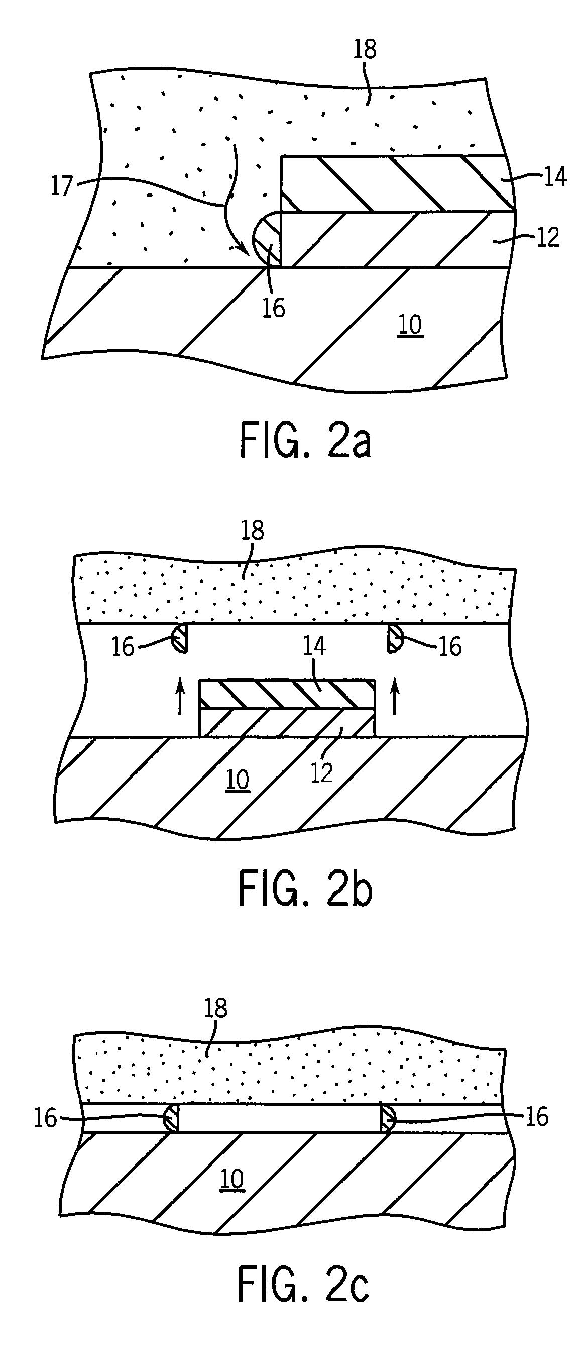
[0007]The present invention provides a method of fabricating small-scale conductors and semiconductors using ESED at a step edge formed by a conductive crystalline diamond, including micro, nano and ultra nano crystalline diamond. This diamond may be patterned by common integrated circuit techniques used in a novel manner and producing not only a well-defined edge, allowing precise dimensions and orientation of the wire to be maintained, but also a robust template surface with relatively low cohesion with the wire allowing the wires, once grown, to be removed and transferred to a different substrate.
[0008]This transfer may be done by a transfer pad allowing mass production of patterned wire circuits or devices by a cyclic stamping process. The transfer process further permits the combination of patterned wire elements from multiple templates to provide for complex interconnections among wires that could not be created directly by ESED. The crystalline diamond permits the formation of complex templates having electrically independent conductive elements allowing the material of the wires to be varied along their lengths permitting the generation of heterogeneous junctions or the like for the production of electronic elements.
[0010]It is thus a feature of at least one embodiment of the invention to provide for the formation of nanoscale wires using a diamond pattern that may have a much larger dimension than the wires. Because only the thickness of the electrode layer determines the minimum wire diameter, the growth time will limit the overall diameter and since the pattern edges define the only the location of the wires and not the diameter, the pattern features can be much wider and still allow wire growth.
[0014]It is thus a feature of at least one embodiment of the invention to provide a simple fabrication process that may use multiple layers of diamond with different doping.

Problems solved by technology

Fabricating devices from nanoconductors can be difficult.
In the above ESED technique, the produced nanowires have irregular orientation resulting from the difficulty of controlling the geometry of the step edges on the HOPG substrate.
Production of the nanowires is further hampered by the fragile nature and expense of the HOPG.
HOPG also contains numerous defects that result in particles forming in between the wires.

Method used


Image

  • Nanowire and microwire fabrication technique and product
  • Nanowire and microwire fabrication technique and product
  • Nanowire and microwire fabrication technique and product

Examples


example i

[0053]It is believed that template of the substrate 10 layer 12 and insulating layer 14, produced as described, can be placed in a bath of 5 millimolar sodium tungstate solution with the conductive layer 12 biased at −1.11 volts with respect to the surrounding solution using an electrode in contact with the solution. The voltage may be applied in short pulses according to constant voltage “stop run chronoamperometry” techniques. The wires can then be reduced in a reduction atmosphere of hydrogen heated to 850 degrees Celsius to produce a pure metal.

[0054]Wires having a thickness of substantially 10 nm and thousands of nanometers in length have been produced in this fashion using Highly Oriented Pyrolytic Graphite instead of UNCD. To date this technique has been used to successfully produce wires from cobalt (using an ionic liquid), copper, tellurium, lead, and gold, zinc, platinum, palladium, cadmium, cadmium telluride, cadmium sulfide and zinc sulfide. It is anticipated that this t...


PUM

PropertyMeasurementUnit
thicknessaaaaaaaaaa
lengthaaaaaaaaaa
lengthaaaaaaaaaa

Abstract

A method of fabricating nanowires or microwires employs a robust conductive surface whose edges define electrodes for promoting electrochemical deposition of nanowire material at those edges. Controlled deposition times and thin conductive layers allow extremely small diameter wires to be created and then removed without destruction of the pattern and the wires to be applied to a second substrate or used for composite materials.

Description

STATEMENT REGARDING FEDERALLY SPONSORED RESEARCH OR DEVELOPMENT[0001]Non ApplicableCROSS REFERENCE TO RELATED APPLICATION[0002]This application claims the benefit of U.S. provisional applications 61 / 023,280 filed Jan. 24, 2008; 61 / 033,580 filed Mar. 4, 2008; 61 / 073,171 filed Jun. 17, 2008; 61 / 081, 241 filed Jul. 16, 2008; and 61 / 088,415 filed Aug. 13, 2008 all hereby incorporated by reference.BACKGROUND OF THE INVENTION[0003]The present invention relates generally to nanotechnology and in particular to a method of creating metallic and semiconducting nanowires, heterogeneous nanowires, and nanowire assemblies using a technique suitable for mass production.[0004]Conductive, semi-conductive, and insulating nanowires hold great promise for the creation of new devices including small-scale electrical circuit elements, sensors, and the like. Of particular interest in this regard are metallic nanowires. The creation of relatively long molybdenum nanowires is described in a paper authored ...

Claims


Application Information

Patent Timeline
Patent Type & Authority Applications(United States)
IPC IPC(8): H01L31/02C25D5/00B32B38/00B32B3/10H01B5/02B23B27/20
CPCC25D1/10H01L31/18Y10T428/24777B23B27/148B82Y30/00B23B2226/31C25D1/04Y10T428/24802B23B2226/27Y02E10/50B23B2210/04B23B2228/44Y10T408/564H01L31/04Y10T428/24851
Inventor ZACH, MICHAEL
Owner WISYS TECH FOUND
Learn More