
Production Method of Group III Nitride Semiconductor Element

a production method and semiconductor technology, applied in semiconductor devices, semiconductor lasers, lasers, etc., can solve the problems of difficult growth of nitride single crystals, failure of epitaxial films to exhibit good crystallinity, etc., to reduce the amount of iii group raw materials, increase the growth temperature excessively, and reduce the growth rate

Inactive Publication Date: 2009-06-04
SHOWA DENKO KK
View PDF3 Cites 5 Cited by
  • Summary
  • Abstract
  • Description
  • Claims
  • Application Information

AI Technical Summary

Benefits of technology

[0044]The reduced growth rate is preferably less than 1 μm / hr. If the reduced growth rate is not less than 1 μm / hr, an effect on improvement in a surface flatness cannot be obtained. The reduced growth rate is more preferably not more than 0.7 μm / hr, and most preferably not more than 0.5 μm / hr. Note that, in the present invention, examples of the reduced growth rate include 0. Even if the reduced growth rate is 0, an advantage of the present invention can be obtained. In this case, the reduction of the growth rate of the semiconductor means interruption of the semiconductor growth. In fact, if the growth rate is set to be 0 and the semiconductor growth is interrupted, a more excellent electrostatic discharge property can be obtained.
[0045]Any method can be used as a method for reducing the growth rate. Examples of the method include reducing an amount of a III group raw material, increasing a growth temperature excessively, increasing a flow rate of a carrier gas, etc. Among these, reducing an amount of a III group material is preferably used. A nitrogen source could be reduced at the same time. However, if the nitrogen source is reduced, the semiconductor grown previously might be decomposed. Accordingly, it is preferable to continue supplying the nitrogen source above a certain level during reducing the growth rate. A flow rate of the nitrogen source, such as NH3, is preferably 1 to 20 litter / min. If the flow rate of the nitrogen source is not more than 1 litter / min, the semiconductor grown previously might be decomposed. If the flow rate of the nitrogen source is more than 20 litter / min, the difference of the advantage is small and only the cost increases. The flow rate of the nitrogen source is more preferably 3 to 18 litter / min and most preferably 5 to 15 litter / min. A flow rate ratio to a carrier gas is preferably less than 1, more preferably less than 2 / 3, most preferably less than 1 / 2.
[0046]Similarly, the growth interruption is preferably carried out by stopping supplying the III group raw material. The nitrogen source could be reduced at the same time. However, if the nitrogen source is reduced, the semiconductor grown previously might be decomposed. Accordingly, it is preferable to continue supplying the nitrogen source during interrupting the growth. The flow rate of the nitrogen source, such as NH3, was mentioned above.
[0047]A carrier gas is preferably a mixture gas of H2 and N2 in the same way as general growth of n-type layer. An H2-riched gas, (namely, a flow rate ratio of H2 to N2 is more than 1), is preferred, because crystallinity of a semiconductor to be formed is improved. The flow rate ratio of H2 to N2 is more preferably more than 1.5 and most preferably more than 2.
[0048]In short, the reduction of the semiconductor growth rate is preferably carried out by continuing flowing a carrier gas and a nitrogen source and reducing an amount of a III group raw material.
[0049]The substrate temperature during reducing the growth rate is preferably kept not lower than the substrate temperature in the course of growth of an n-type layer immediately before the growth rate is reduced. If the substrate temperature during reducing the growth rate is lower than the substrate temperature in the course of growth of an n-type layer immediately before the growth rate is reduced, the electrostatic discharge property is less improved. The substrate temperature during reducing the growth rate is preferably 900 to 1400° C. If the substrate temperature is less than 900° C., the electrostatic discharge property is less improved. If the substrate temperature is more than 1400° C., crystallinity of a semiconductor layer grown previously is deteriorated or surface flatness of a semiconductor layer grown previously is reduced, thus resulting in the deterioration in crystallinity of a semiconductor layer formed thereon.

Problems solved by technology

Growing only a nitride single crystal itself has been considered difficult, for the following reasons.
However, even when a nitride semiconductor single crystal is grown directly on such a single-crystal substrate, many crystal defects, which are attributed to crystal lattice mismatch between the crystalline substrate and the single crystal, are generated in the resultant nitride semiconductor single crystal film; i.e., the epitaxial film fails to exhibit good crystallinity.

Method used


Image

  • Production Method of Group III Nitride Semiconductor Element
  • Production Method of Group III Nitride Semiconductor Element

Examples


example 1

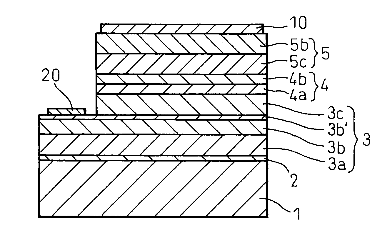
[0059]FIG. 2 is a schematic diagram showing the cross-sectional structure of the Group III nitride semiconductor light-emitting device fabricated in this example.

[0060]A stacked structure including a sapphire substrate 1 and Group III nitride semiconductor layers successively stacked on the substrate 1 was formed by means of conventional low-pressure MOCVD through the following procedure. Firstly, a (0001)-sapphire substrate 1 was placed on a high-purity graphite (for semiconductor) susceptor to be heated at a film formation temperature by a high-frequency (RF) induction heater. The sapphire substrate placed on the susceptor was placed in a stainless steel-made vapor-phase epitaxy reactor, and the reactor was purged with nitrogen.

[0061]After passage of nitrogen in the vapor-phase epitaxy reactor for 8 minutes, the substrate 1 was heated over 10 minutes from room temperature to 600° C. by means of the induction heater. While the substrate 1 was maintained at 600° C., hydrogen gas and...

example 2

[0076]A light-emitting device of a Group III nitride semiconductor was formed in a similar way to Example 1, except that, after the n-type contact layer 3b was grown, supplying of TMG and (CH3)4Ge into a vapor-phase epitaxy reactor was completely stopped, without changing the growth temperature, the flow rate of a carrier gas and the flow rate of an ammonia gas. Therefore, there was no reduced-growth-rate layer 3b′ in this example.

[0077]The obtained light-emitting device was evaluated in the same manner as in Example 1. The chip exhibited forward voltage of 3.5 V at a forward current of 20 mA. The emission peak wavelength of the band of blue light emission at a forward current of 20 mA was found to be 460 nm. The emission intensity of the light emitted from the chip, as determined through a typical integrating sphere, was 5 mW. Thus, a Group III nitride semiconductor light-emitting device attaining a high emission intensity was successfully fabricated. In the electrostatic discharge...

example 3

[0078]A Group III nitride semiconductor light-emitting device was formed in a similar way to example 2, except that after an n-type contact layer was grown to half of the total thickness, i.e., after 50 cycles, each cycle consisting of supply of tetramethyl germanium ((CH3)4Ge) for 18 seconds and interruption of supply for 18 seconds, were repeatedly conducted, supplying of TMG and ((CH3)4Ge) into a vapor-phase epitaxy reactor was completely stopped for 30 minutes, without changing the growth temperature, the flow rate of a carrier gas and the flow rate of an ammonia gas. Namely, in this example, growth of a semiconductor layer was interrupted twice, during growth and immediately after growth of the n-type contact layer 3b.

[0079]The obtained light-emitting device was evaluated in the same manner as in Example 1. The chip exhibited forward voltage of 3.5 V at a forward current of 20 mA. The emission peak wavelength of the band of blue light emission at a forward current of 20 mA was...


PUM

PropertyMeasurementUnit
thicknessaaaaaaaaaa
temperatureaaaaaaaaaa

Abstract

An object of the present invention is to provide a production method of a Group III nitride semiconductor element having an excellent electrostatic discharge property and enhanced reliability.In the inventive production method, the Group III nitride semiconductor element has an n-type layer, an active layer and a p-type layer, which comprise a Group III nitride semiconductor, on a substrate in this order, wherein, during or / and after growth of the n-type layer and before growth of the active layer, the growth rate of the semiconductor is reduced.

Description

CROSS REFERENCE TO RELATED APPLICATIONS[0001]This application is an application filed under 35 U.S.C. §111(a) claiming benefit, pursuant to 35 U.S.C. §119(e)(1), of the filing date of the Provisional Application No. 60 / 671,494 filed on Apr. 15, 2005 and of the Provisional Application No. 60 / 683,308 filed on May 23, 2005, pursuant to 35 U.S.C. §111(b).TECHNICAL FIELD[0002]The present invention relates to a production method of a Group III nitride semiconductor element which exhibits good reliability and which is employed in, for example, light-emitting diodes, laser diodes, and light-receiving devices.BACKGROUND ART[0003]Group III nitride semiconductors have a direct transition band structure and exhibit bandgap energies corresponding to the energy of visible to ultraviolet light. By virtue of these characteristics, Group III nitride semiconductors are employed at present for producing light-emitting devices, including blue LEDs, blue-green LEDs, ultraviolet LEDs, and white LEDs whic...

Claims


Application Information

Patent Timeline
Patent Type & Authority Applications(United States)
IPC IPC(8): H01L33/00H01L21/20H01L29/20H01L33/06
CPCB82Y20/00H01L21/0237H01L21/02458H01L21/0254H01S2304/04H01L21/0262H01L33/007H01S5/34333H01L21/02573H01L21/0242H01L21/02576H01L21/02579H01L33/06H01S5/32341
Inventor TAKEDA, HITOSHI
Owner SHOWA DENKO KK
Learn More