
Random Access Electrically Programmable E-Fuse Rom

a random access, electrically programmable technology, applied in the direction of static storage, digital storage, instruments, etc., can solve the problems of significant failure mechanisms of fuse regrowth, blown fuses and fuse regrowth, and difficulty in both supply, so as to reduce the applied voltage, reduce the resistance, and reduce the time

Active Publication Date: 2008-12-25
IBM CORP
View PDF6 Cites 36 Cited by
  • Summary
  • Abstract
  • Description
  • Claims
  • Application Information

AI Technical Summary

Benefits of technology

[0010]It is therefore an object of the present invention to provide an e-fuse array structure for enabling a fuse blow with both current and voltage to successfully migrate silicide from the fuse link without blowing or rupturing the polysilicon of the fuse link.
[0011]It is another object of the present invention to provide an e-fuse array structure for enabling a highly reliable e-fuse system by avoiding a partial or ruptured fuse blow condition which can result in a significant failure mechanism for the fuse link.
[0013]It is yet another object of the invention to provide an e-fuse array which is modular and expandable while providing enhanced protection on e-fuse cells from damage due to programming of physically or electrically adjacent e-fuse cells and which is reliably field-programmable.
[0015]It is yet another further object of the invention to provide a programmable e-fuse array capable of providing enhanced operating margins for read operations.
[0018]The invention provides a novel non-volatile memory as a system through aggressive scaling of fuse link dimensions and geometry, allowing decreased resistance in both the fuse link and the programming circuitry which, in turn allows reliable programming to be performed in much reduced time at relatively lower applied voltages and reduced current and which can be supplied from an on-chip power supply such as a charge pump to support field programming of the memory. Such an on-chip selection and level shifting circuit for both write and read modes of the memory also provides protection of non-selected cells during write operations. The aggressively scaled fuse link provides a significant size reduction over known designs while use of single bit line sensing and use of a shared, tunable reference for a tunable sense amplifier for each bit line, rather than a sense amplifier for each fuse link, provides additional reduction in cell size and increase in effective storage cell density by a factor of about twenty over known designs while tunability of the reference source and sense amplifier can compensate for chip-to-chip manufacturing variations and optimize operating margins. Thus, a non-volatile memory of improved functionality and reliability and capable of storing a practical amount of data comparable with other non-volatile memory structures can be provided in a two-dimensional array on a single chip; greatly increasing the number of applications and uses to which the memory in accordance with the invention may be applied. By the same token, the reduction in cell size of the memory in accordance with the invention allows additional features such as error correction code (ECC) facilities, redundant circuits, such as for improving manufacturing yield or providing for apparent multiple write capabilities, can be provided. Defective e-fuses and defective sense amplifiers can also be detected during manufacture.

Problems solved by technology

However, device densities are limited because of problems of scalability.
In addition, while these known conventional OTPROM approaches which blow the fuse by applying a large current to the selected device can initially be programmed successfully, partially blown fuses and fuse regrowth are significant failure mechanisms because of fully or partially migrated fuse links.
Use of such a high current and voltage also implies difficulty in both supplying an adequately large voltage to develop adequate programming currents due to a large IR voltage drop due to resistance in the fuse programming circuit and in integration of fuses as an array and / or with other circuits on an integrated circuit chip due to the requirement for a large area of the integrated circuit of approximately 100 μm2 / fuse due to the 5.2 nm gate oxide in the fuse element / blow device and a high voltage protection device for other elements in the fuse circuit.
Further, when using high programming voltages, thick oxide is required in the blow path and to protect sense amplifiers generally provided for individual fuses, thus limiting reduction of the required area for each bit or e-fuse.
Problems of operation have also been encountered using such high voltages and ensuring that only the desired fuse is programmed has also precluded a large 2-D array of e-fuses.
The most important issue for an e-fuse based OTPROM is to enable an embedded application.
These embedded system-related issues have not been addressed for any known OTPROM.

Method used


Image

  • Random Access Electrically Programmable  E-Fuse Rom
  • Random Access Electrically Programmable  E-Fuse Rom
  • Random Access Electrically Programmable  E-Fuse Rom

Examples


Embodiment Construction

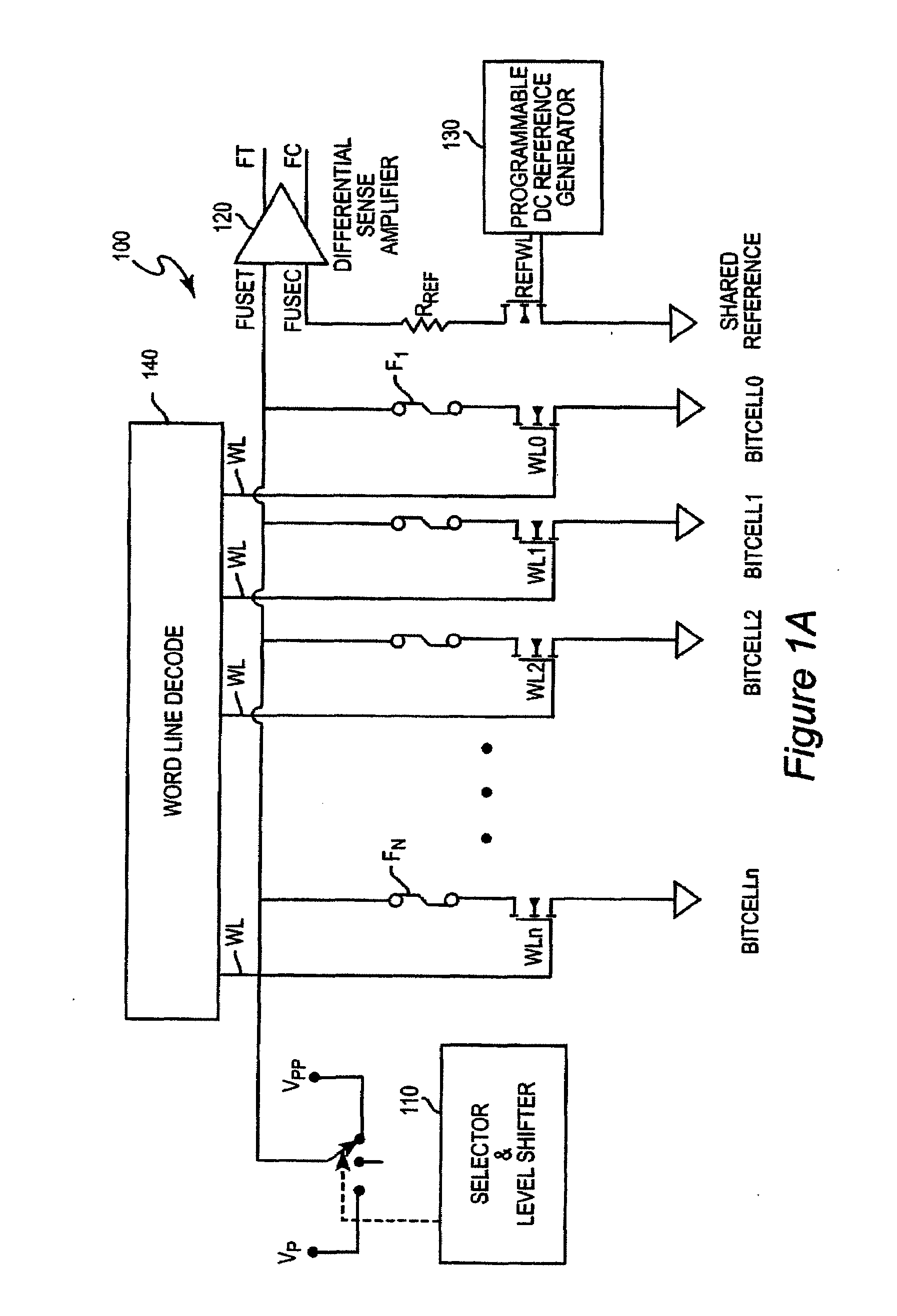
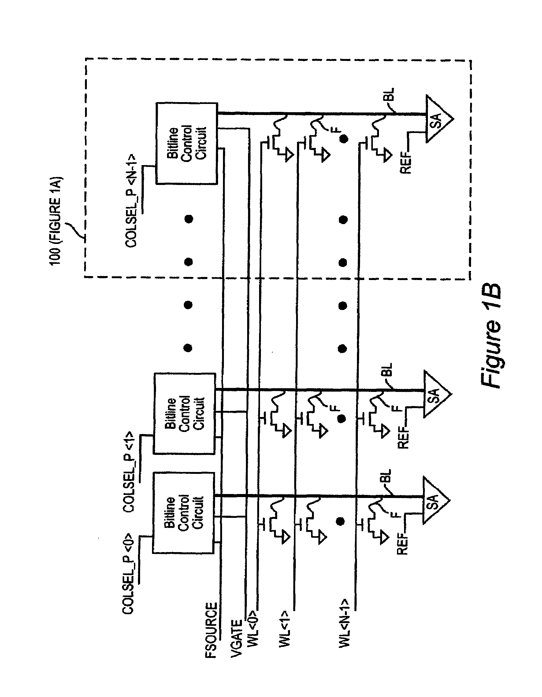
[0027]Referring now to the drawings, and more particularly to FIG. 1A, there is shown a schematic diagram of a portion of the programmable array of e-fuses corresponding to a bit line (BL) and suitable for use as a read only memory (ROM) in accordance with the invention. The portion 100 of the array illustrated in FIG. 1A corresponds to a column of FIG. 1B, as shown by a dashed line box illustrated therein. Some similarity of FIG. 1A to schematic depictions of known e-fuse arrays and memory arrays will be recognized by those skilled in the art. However, the schematic illustration of FIG. 1A employs a unique configuration to reliably blow the silicide in the fuse links without rupturing the polysilicon fuse links and to detect the fuse resistance reliably as controlled by the word line and bit line.

[0028]Similarly to a conventional memory array structure, while selection is performed by simultaneous energization of a bit line (BL) and a word line (WL), a transistor (preferably an NMO...


PUM


Abstract

A one-time-programmable-read-only-memory (OTPROM) is implemented in a two-dimensional array of aggressively scaled suicide migratable e-fuses. Word line selection is performed by decoding logic operating at VDD while the bit line drive is switched between VDD and a higher voltage, Vp for programming. The OTPROM is thus compatible with and can be integrated with other technologies without a cost adder and supports optimization of the high current path for minimal voltage drop during fuse programming. A differential sense amplifier with a programmable reference is used for improved sense margins and can support an entire bit line rather than sense amplifiers being provided for individual fuses.

Description

BACKGROUND OF THE INVENTION[0001]1. Field of the Invention[0002]The present invention generally relates to read only memories comprised of e-fuses and, more particularly, to large capacity, field-programmable, one-time programmable read only memories (OTPROMs) comprised of aggressively scaled e-fuses allowing the OTPROM to be arranged in a two-dimensional (2-D) array.[0003]2. Description of the Prior Art[0004]Electrically programmable fuses (e-fuses) have proven highly reliable and a convenient expedient for many electronic applications such as substitution of redundant circuitry for marginally performing circuitry in complex integrated circuits such as memories to increase manufacturing yield and customization of standard designs for logic circuitry and custom read only memories / decoders. Particularly for the latter types of applications, there is interest in applying e-fuses to one-time-programmable-read-only-memories (OTPROMs) of larger capacity and which can be programmed in the...

Claims


Application Information

Patent Timeline
IPC IPC(8): G11C17/00G11C17/16
CPCG11C17/16G11C29/027G11C17/165G11C7/06G11C7/18G11C17/18G11C29/026G11C2229/763
Inventor FREDEMAN, GREGORY J.KIRIHATA, TOSHIAKILESLIE, ALAN J.SAFRAN, JOHN M.
Owner IBM CORP
Learn More