
Semiconductor interlayer-insulating film forming composition, preparation method thereof, film forming method, and semiconductor device

Inactive Publication Date: 2008-11-27
PANASONIC CORP +1
View PDF12 Cites 32 Cited by
  • Summary
  • Abstract
  • Description
  • Claims
  • Application Information

AI Technical Summary

Benefits of technology

[0012]A number of attempts to develop materials for forming a low-dielectric-constant insulating film having both a low dielectric constant and high mechanical strength including the above-described technologies have been made, but materials capable of satisfying both of them have not yet been found. For example, in an attempt to use zeolite fine particles, the mechanical strength of the film is much inferior to that expected from the mechanical strength of zeolite itself so that a new breakthrough is necessary for incorporating fine particles in a film, thereby increasing the mechanical strength thereof.
[0013]With the foregoing in view, one object of the present invention is to provide a novel coating solution for forming porous-film which can easily provide, by a method ordinarily employed in a conventional semiconductor manufacturing method, a thin film having a freely controlled thickness and excellent in both mechanical strength and dielectric properties. Another object of the invention is to provide a high-performance and high-reliability semiconductor device having therein the porous film.
[0014]The present inventors have carried out an extensive investigation with a purpose of developing a coating solution for forming porous-film having the above-described properties. As one attempt, they make a working hypothesis that if a bond between silicon-oxide-based fine particles constituting the skeleton of a porous film can be reinforced at a soft sintering step before sintering, shrinkage of the film during sintering can be suppressed and a sufficient porosity can be maintained by spaces formed between these particles; and since the skeleton is not broken, the porous film can have improved mechanical strength. They searched for materials capable of reinforcing the bond between particles and serving as a so-called adhesive.

Problems solved by technology

A number of attempts to develop materials for forming a low-dielectric-constant insulating film having both a low dielectric constant and high mechanical strength including the above-described technologies have been made, but materials capable of satisfying both of them have not yet been found.

Method used


Image

  • Semiconductor interlayer-insulating film forming composition, preparation method thereof, film forming method, and semiconductor device
  • Semiconductor interlayer-insulating film forming composition, preparation method thereof, film forming method, and semiconductor device
  • Semiconductor interlayer-insulating film forming composition, preparation method thereof, film forming method, and semiconductor device

Examples


preparation example 1

[0148]A mixture of 45 g of methyltrimethoxysilane and 101 g of tetraethoxysilane was added, under stirring at room temperature, to a solution obtained by dissolving 0.18 g of concentrated nitric acid in 280 g of ultrapure water. The reaction mixture gradually generated heat and reached 50° C. but 30 minutes later, it returned to room temperature. Stirring was continued for 12 hours without changing the condition. To the reaction mixture was added 300 g of propylene glycol monomethyl ether acetate (which will hereinafter be referred to as PGMEA) and the low-boiling-point solvent was distilled off under reduced pressure. During this distillation, a bath of the evaporator was kept at 30° C. or less. To the remaining solution thus obtained were added 500 ml of toluene and 500 ml of ultrapure water. The resulting mixture was transferred to a separating funnel so as to remove a water layer. The organic layer was washed twice with 200 ml of ultrapure water. The organic layer thus obtained ...

preparation example 2

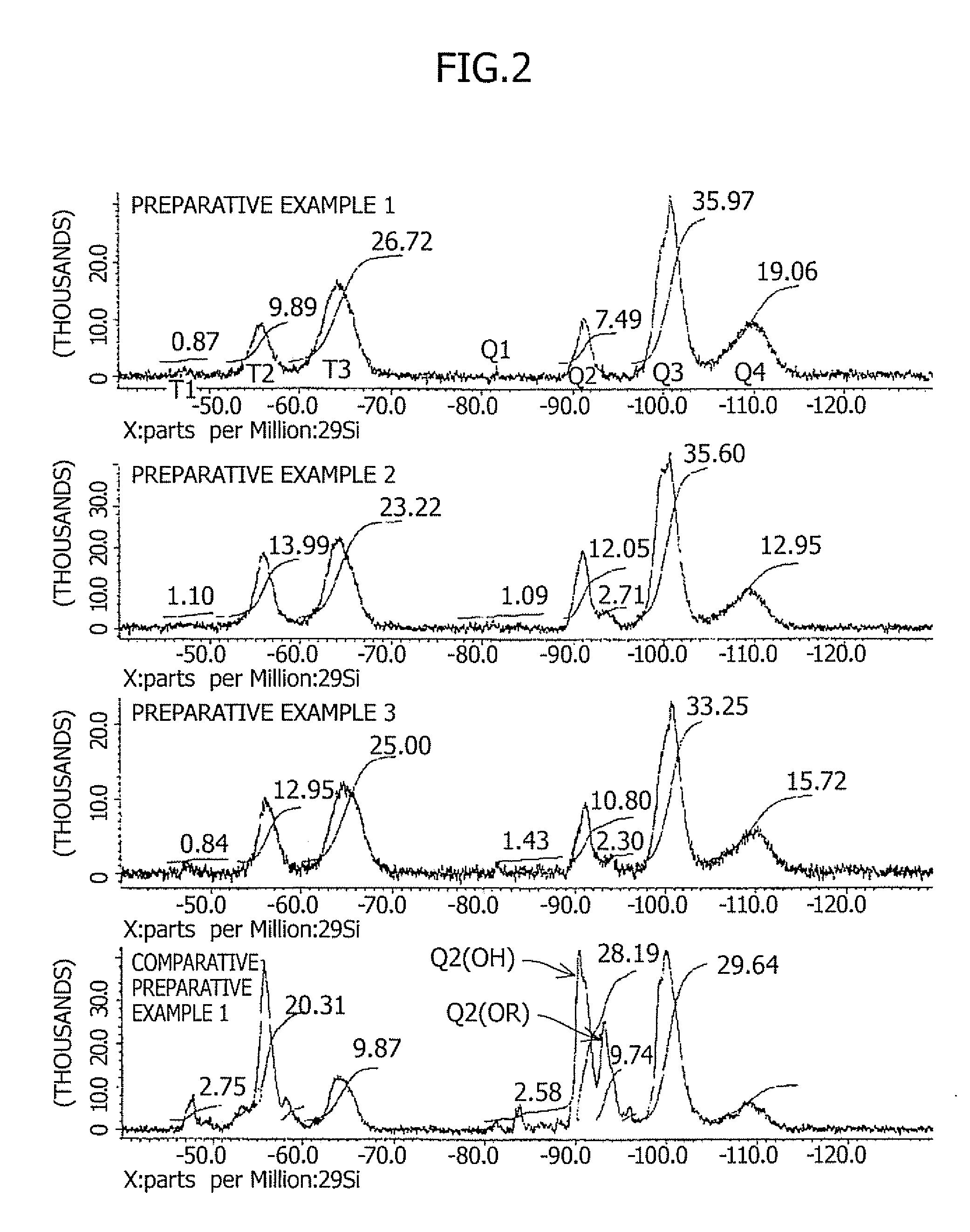
[0150]In a similar manner to Preparation Example 1 except for the use of 0.11 g of concentrated sulfuric acid instead of nitric acid, synthesis was conducted, whereby 205 g of a concentrated solution was obtained. The resulting solution had a nonvolatile residue of 22.4 mass % and a weight average molecular weight, as determined by GPC, of 3,522. As a result of the 29Si—NMR measurement of the sample, it has been found that the molar ratios t1, t2, t3, q1, q2, q3 and q4 were 1%, 14%, 23%, 1%, 12%, 36%, and 13%, respectively and calculation using these ratios resulted in the following relationships:

(q1+q2+t1) / (q1+q2+q3+q4+t1+t2+t3)=0.16 and

(q3+t2) / (q1+q2+q3+q4+t1+t2+t3)=0.50.

preparation example 3

[0151]In a similar manner to Preparation Example 1 except for the use of 0.31 g of concentrated hydrochloric acid instead of nitric acid, synthesis was conducted, whereby 213 g of a concentrated solution was obtained. The resulting solution had a nonvolatile residue of 20.6 mass % and a weight average molecular weight, as determined by GPC, of 1,988. The 29Si—NMR measurement of the sample was performed. As a result, it has been found that calculation based on the molar ratios t1, t2, t3, q1, q2, q3 and q4 leads to the following relationships:

(q1+q2+t1) / (q1+q2+q3+q4+t1+t2+t3)=0.12 and

(q3+t2) / (q1+q2+q3+q4+t1+t2+t3)=0.46.


PUM

PropertyMeasurementUnit
Dimensionless propertyaaaaaaaaaa
Dielectric polarization enthalpyaaaaaaaaaa
Compositionaaaaaaaaaa

Abstract

Provided is a porous-film-forming composition containing silicon-oxide-based fine particles and a polysiloxane compound obtained by hydrolysis and condensation reactions, in the presence of an acid catalyst, of a hydrolyzable silane compound containing at least one tetrafunctional alkoxysilane compound represented by the following formula (1):Si(OR1)4  (1)wherein, R1s may be the same or different and each independently represents a linear or branched C1-4 alkyl group and / or at least one alkoxysilane compound represented by the following formula (2):R2nSi(OR3)4-n  (2)wherein, R2(s) may be the same or different when there are plural R2s and each independently represents a linear or branched C1-8 alkyl group, R3(s) may be the same or different when there are plural R3s and each independently represents a linear or branched C1-4 alkyl group, and n is an integer from 1 to 3 in the reaction mixture containing a large excess of water.

Description

CROSS-RELATED APPLICATIONS[0001]This application claims priority from Japanese Patent Application No. 2007-036343; filed Feb. 16, 2007, the disclosure of which is incorporated herein by reference in its entirety.BACKGROUND OF THE INVENTION[0002]1. Field of the Invention[0003]The present invention relates to a film forming composition capable of providing a porous film excellent in dielectric properties and mechanical strength, a method for forming a porous film, a porous film thus formed, and a semiconductor device having therein the porous film.[0004]2. Description of the Related Art[0005]In the fabrication of semiconductor integrated circuits, as their integration degree becomes higher, an increase in interconnect delay time due to an increase in interconnect capacitance, which is a parasitic capacitance between metal interconnects, prevents their performance enhancement. The interconnect delay time is called an RC delay which is in proportion to the product of electric resistance...

Claims


Application Information

Patent Timeline
IPC IPC(8): H01L23/58C08K3/34C08K3/36B32B5/18H01L21/312
CPCC08G77/16C08G77/70C08G77/80C08K3/36C08L83/04C09D183/04H01L21/02126H01L21/02203H01L21/02216H01L21/02282H01L21/3122H01L21/31695H01L21/7682C08L83/00H01L2221/1047Y10T428/249953H01L21/31H01L21/3205
Inventor YAGIHASHI, FUJIOHAMADA, YOSHITAKAASANO, TAKESHIOGIHARA, TSUTOMUIWABUCHI, MOTOAKINAKAGAWA, HIDEOSASAGO, MASARU
Owner PANASONIC CORP
Learn More