Conductive film and method for manufacturing the same

Inactive Publication Date: 2008-11-13
MURATA MFG CO LTD
View PDF7 Cites 27 Cited by
  • Summary
  • Abstract
  • Description
  • Claims
  • Application Information

AI Technical Summary

Benefits of technology

[0040]By forming a third ZnO conductive film layer being transparent, containing a Group III oxide as a dopant that is different to the Group III oxide contained in the second ZnO conductive film layer, and formed on the second ZnO conductive film layer, other desired properties can be imparted to the conductive film layer composed of a conductive film (a second ZnO conductive film layer) having high moisture resistance, high orientation, and transparency. This results in the present invention being more effective.
[0043]It is also found that when two or more ZnO conductive film layers containing a Group III oxide as a dopant different to the Group III oxide contained in adjacent conductive film layers are formed on the second ZnO conductive film layer, the high crystallinity of the second ZnO conductive film layer can also be obtained in the following ZnO conductive film layer.
[0045]Furthermore, if the first ZnO conductive film layer has a thickness of 5 to 50 nm, the ZnO conductive film layer having high crystallinity and moisture resistance can be preferably obtained.
[0047]When the thickness of the first ZnO conductive film layer exceeds 50 nm, the thicknesses of the second and following ZnO conductive film layers become relatively small if the total thickness of the conductive film is constant which may cause problems, so that the desired properties cannot be obtained. Therefore, it is preferable that the thickness of the first ZnO conductive film layer be less than 50 nm.
[0048]That is, in the present invention, since the first ZnO conductive film layer is formed considering improvement of crystallinity, orientation, and moisture resistance of the second and following ZnO conductive film layers formed on the first ZnO conductive film layer rather than considering properties such a low electric resistivity, if the thickness of the first ZnO conductive film layer can be reduced to 50 nm or less, an improvement of the properties such as moisture resistance can preferably be achieved without losing any suitable properties such as low electric resistivity of the entire conductive film.
[0049]Furthermore, the function of the first ZnO conductive film layer, which improves the crystallinity and orientation of the second ZnO conductive film layer and following conductive film layers, can be sufficiently realized by regulating the content of Group III oxide in the second and following ZnO conductive film layers other than the first ZnO conductive film layer to 7 wt % or less. Therefore, a suitable conductive film having suitable properties can be obtained without fail.
[0050]Note that if the doping content of the Group III oxide is increased, the electric resistivity is relatively increased. If the doping content exceeds 7 wt %, the electric resistivity is increased and problems occur in practical use. Therefore, the content of the Group III oxide is preferably 7 wt % or less.
[0046]Note that if the thickness of the first ZnO conductive film layer comes to less than 5 nm, the high crystallinity obtained for the first ZnO conductive film layer may not be sufficiently obtained for the second ZnO conductive film layer. Therefore, it is preferable that the thickness of the first ZnO conductive film layer be 5 nm or more.
[0053]In the present invention, a substrate having a main component including at least one material selected from the group composed of glass, quartz crystal, sapphire, silicon, silicon carbide, polyethylene terephthalate, polyethylene naphthalate, polyethersulfone, polyimide, cycloolefin polymer, and polycarbonate can be used, and according to the present invention, a ZnO-based conductive film having moisture resistance for practical use and an advantage in terms of economical efficiency can be formed on the substrate composed of the above-mentioned materials.
[0054]In the present invention, each of the ZnO conductive film layers can be formed by a method selected from the group composed of sputtering, vapor deposition, evaporation ion plating, laser ablation, arc plasma vapor deposition, and plating. Accordingly, a conductive film having high moisture resistance and high orientation, that is, a conductive film having advantageous properties can be efficiently manufactured.
[0057]Furthermore, when the first ZnO conductive film layer is formed by a method selected from the group composed of sputtering, vapor deposition, evaporation ion plating, laser ablation, arc plasma vapor deposition, and plating while applying heat treatment to the first ZnO conductive film layer during the formation thereof and then the second and following ZnO conductive film layers are formed on the first ZnO conductive film layer by a method selected from the group composed of sputtering, vapor deposition, evaporation ion plating, laser ablation, arc plasma vapor deposition, and plating while applying heat treatment or no heat treatment during the formation thereof, the high crystallinity obtained for the first ZnO conductive film layer can also be efficiently obtained for the second ZnO conductive film layer and following conductive film layer without fail. That results in the present invention being more effective.
[0056]Note that when two or more ZnO conductive film layers containing a Group III oxide as a dopant different to the Group III oxide contained in adjacent conductive film layers are further formed on the second ZnO conductive film layer, the high crystallinity of the second ZnO conductive film layer can be obtained in the following ZnO conductive film layer and a conductive film having desired properties and a multi-layer structure of three layers or more can be efficiently manufactured.
[0057]Furthermore, when the first ZnO conductive film layer is formed by a method selected from the group composed of sputtering, vapor deposition, evaporation ion plating, laser ablation, arc plasma vapor deposition, and plating while applying heat treatment to the first ZnO conductive film layer during the formation thereof and then the second and following ZnO conductive film layers are formed on the first ZnO conductive film layer by a method selected from the group composed of sputtering, vapor deposition, evaporation ion plating, laser ablation, arc plasma vapor deposition, and plating while applying heat treatment or no heat treatment during the formation thereof, the high crystallinity obtained for the first ZnO conductive film layer can also be efficiently obtained for the second ZnO conductive film layer and following conductive film layer without fail. That results in the present invention being more effective.
[0058]That is, by applying a heat treatment, the first ZnO conductive film layer having high crystallinity can be surely formed. Although the second ZnO conductive film layer may be formed by applying heat treatment, the second ZnO conductive film layer can also be formed under room temperature without applying heat treatment because the high crystallinity and the other properties obtained for the first ZnO conductive film layer may also be obtained for the second ZnO conductive film layer. This results in a highly efficient manufacturing process.
[0059]There are other methods for forming the first ZnO conductive film layer having high crystallinity other than heat treatment. Examples of these methods include optimizations of pressure, doping content, dopant species, power supply, and bias power applied to a substrate.

Problems solved by technology

However, since indium is expensive and an exhaustible resource, transparent electrodes have been increasingly required to be composed of materials other than indium.
However, ZnO-based transparent conductive films have the problem that the moisture resistance thereof is insufficient in practical use.
That is, since the existing ZnO-based transparent conductive films have considerable oxygen vacancy, when placed under a high humidity condition, a decrease in carrier concentration due to adsorption of water (reoxidation) to places where oxygen are absent disadvantageously leads to a high electric resistance.
However, ZnO-based transparent conductive films satisfying the rough standard have not yet been obtained.
Furthermore, if ZnO-based transparent conductive films are formed on flexible substrates that will be used in many applications in the future, since moisture can penetrate the flexible substrate, the ZnO-based transparent conductive films are further disadvantageously deteriorated because not only moisture penetrating from a surface of the transparent conductive films but also moisture penetrating through the flexible substrates negatively affects the ZnO-based transparent conductive films.
As of now, however, ZnO-based transparent conductive films having practicable moisture resistance cannot be obtained.
The ZnO-based transparent conductive films mentioned above actually have the same problems, to some extent, with respect to moisture resistance mentioned above.

Method used


Image

  • Conductive film and method for manufacturing the same
  • Conductive film and method for manufacturing the same
  • Conductive film and method for manufacturing the same

Examples


example 1

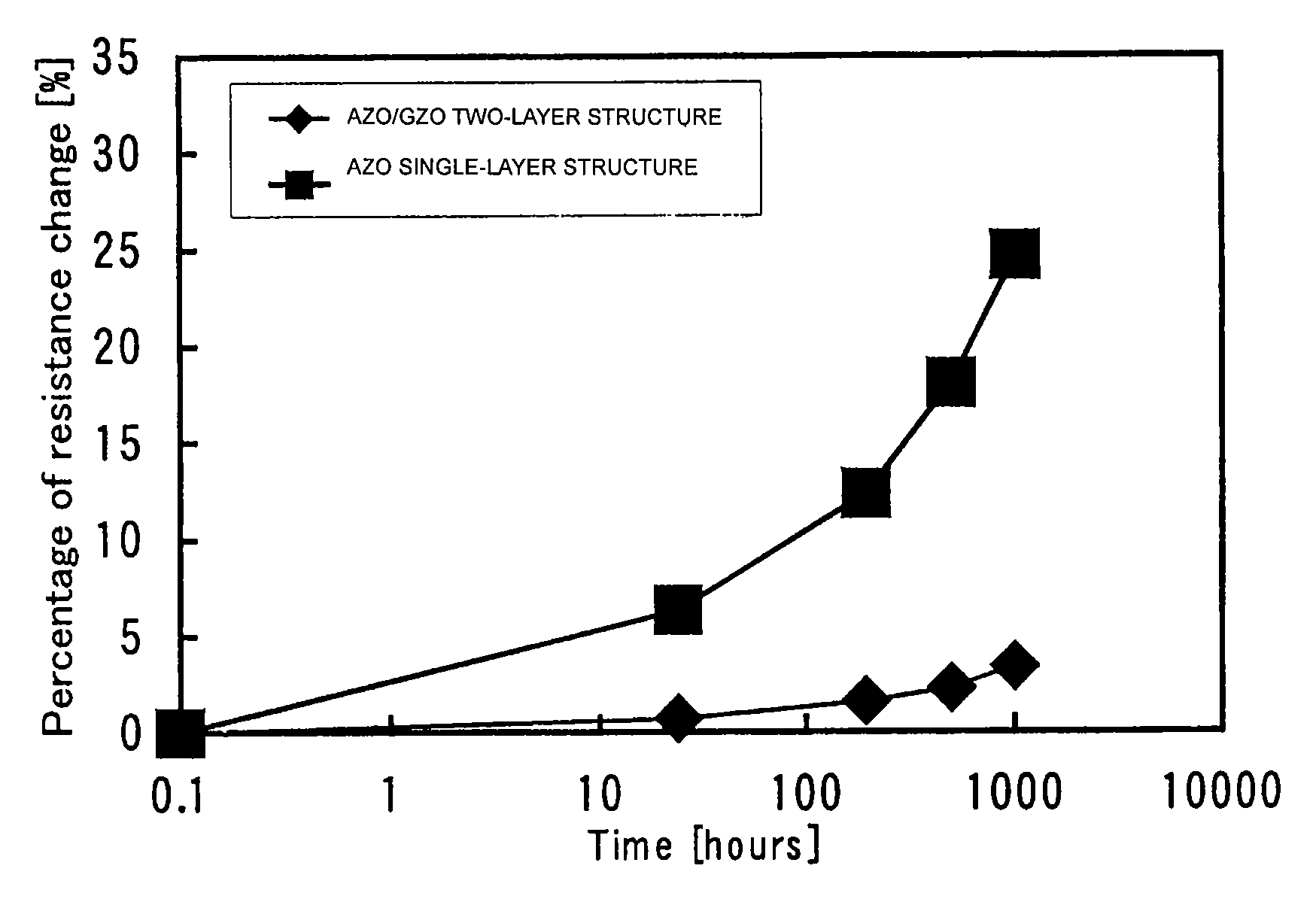
[0087]FIG. 6 is a view of a conductive film formed on a substrate according to an example (EXAMPLE 1) of the present invention.

[0088]As shown in FIG. 6, a conductive film 10 of EXAMPLE 1 has a two-layer structure composed of a first ZnO conductive film layer 1 being transparent, formed on a surface of a substrate 11, and including ZnO as a main component and a Group III oxide as a dopant and a second ZnO conductive film layer 2 being transparent, formed on the first ZnO conductive film layer 1, and including a Group III oxide as a dopant different to the Group III oxide included in the first conductive film layer.

[0089]Note that, in EXAMPLE 1, a glass substrate made of alkali-free glass (Corning 1737) was used for the substrate 11.

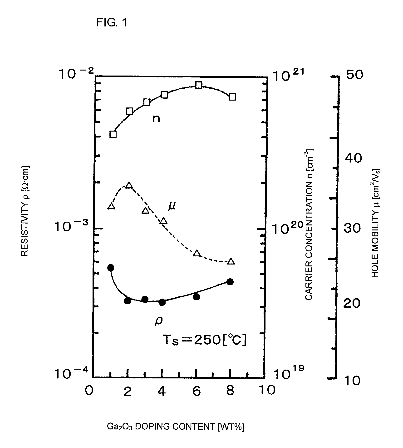
[0090]A ZnO conductive film was formed on a surface of the glass substrate 11 as the first ZnO conductive film layer 1 doped with Ga2O3 as a Group III oxide.

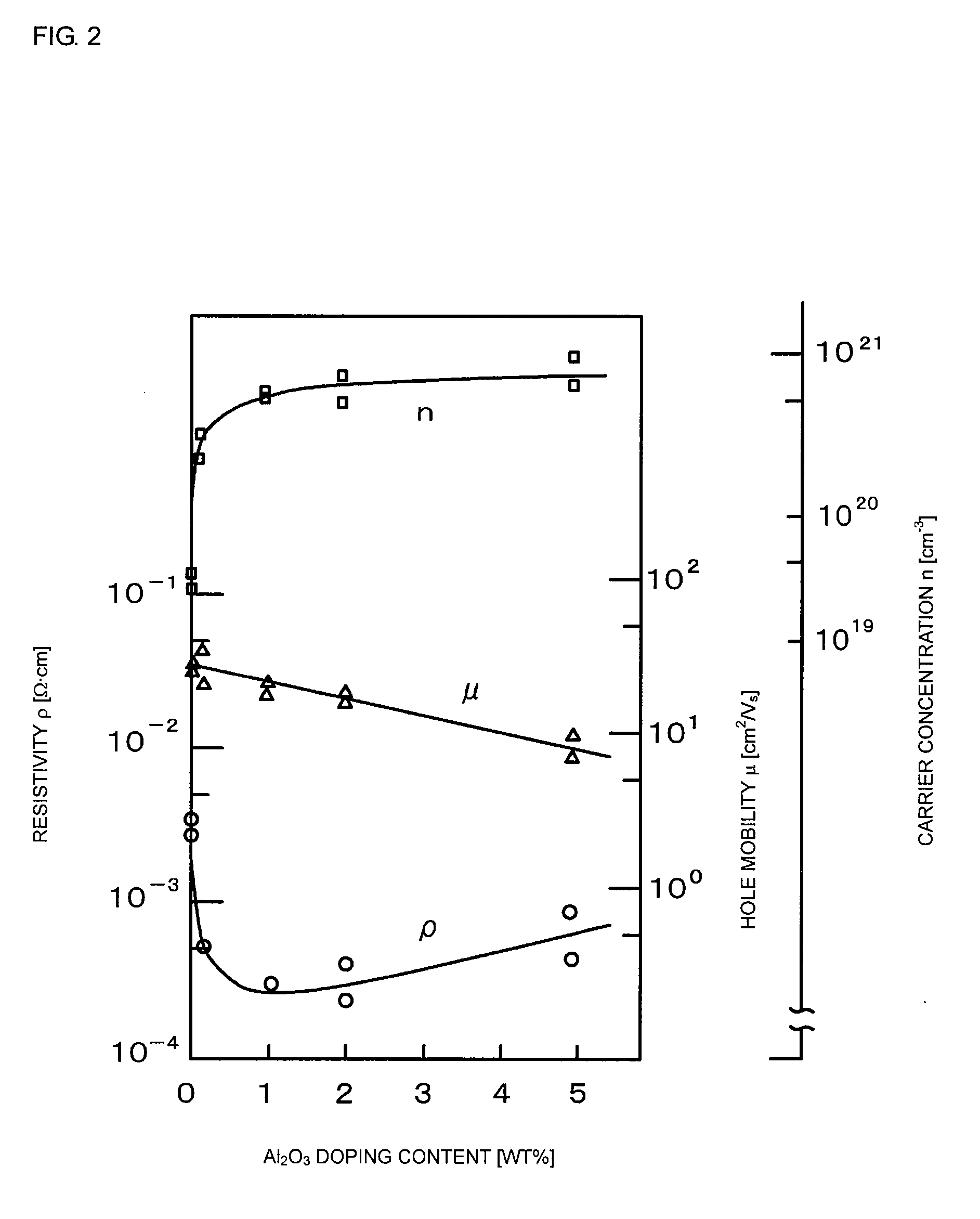
[0091]Furthermore, another ZnO conductive film was formed on the first ZnO conductive film layer 1 ...

example 2

[0113]EXAMPLE 1 describes a case where a glass plate is used as a substrate on which a conductive film is formed. EXAMPLE 2 describes another case where a PEN (polyethylene naphthalate) flexible substrate is used as a substrate on which a conductive film is formed. By a method similar to those used in the above-mentioned EXAMPLE 1, PEN substrates were subjected to a preparation treatment and sputtered under the same conditions as those performed in EXAMPLE 1. An AZO / GZO two-layer structure conductive film and an AZO single-layer structure conductive film were formed on the flexible substrates composed of PEN.

[0114]Properties of each conductive film were investigated using a method similar to those used in the above-mentioned EXAMPLE 1. Measurement results similar to those obtained from EXAMPLE 1 were obtained. It was found that if the conductive film is formed on a flexible substrate composed of PEN, a ZnO conductive film constituted by an AZO / GZO two-layer structure film has high c...

example 3

[0115]EXAMPLE 1 describes a case where a glass plate is used as a substrate on which a conductive film is formed and EXAMPLE 2 describes a case where a PEN flexible substrate is used as a substrate on which a conductive film is formed. EXAMPLE 3 describes another case where a PET (polyethylene terephthalate) flexible substrate is used as a substrate on which a conductive film is formed. By a method similar to those used in the above-mentioned EXAMPLES 1 and 2, PET substrates were subjected to a preparation treatment and sputtered under the same conditions as those performed in EXAMPLE 1. An AZO / GZO two-layer structure conductive film and an AZO single-layer structure conductive film were formed on the flexible substrates composed of PET.

[0116]In EXAMPLE 3, similarly to EXAMPLES 1 and 2, when a flexible substrate composed of PET (polyethylene terephthalate) was used as a substrate, it was found that a ZnO conductive film constituted by an AZO / GZO two-layer structure film has high cry...


PUM

PropertyMeasurementUnit
Thicknessaaaaaaaaaa
Concentrationaaaaaaaaaa
Electrical resistanceaaaaaaaaaa

Abstract

A ZnO-based conductive film having acceptable practical use moisture resistance, properties required for a transparent conductive film, and economical advantage and a method for manufacturing the film are provided. A first ZnO conductive film layer 1, optionally containing a Group III oxide dopant, is formed on a surface of a substrate 11 and a second ZnO conductive film layer 2, which is transparent and includes a Group III oxide different from a Group III oxide (if present) included in the first conductive film layer is formed on the first ZnO conductive film layer to form a multi-layer structure. The thickness of the first ZnO conductive film layer is preferably 5 to 50 nm, and the second and any following ZnO conductive film layers include a Group III oxide at a concentration of 7 wt % or less. The first ZnO conductive film layer is formed under a condition in which high crystallinity can be obtained (for example, under a heat treatment) so as to enhance the crystallinity of the second ZnO conductive film layer and following conductive film layers formed on the first ZnO conductive film layer.

Description

[0001]This is a continuation of application Serial No. PCT / JP2008 / 050806, filed Jan. 22, 2008.TECHNICAL FIELD[0002]The present invention relates to a conductive film and a method for manufacturing the same, specifically, to a conductive film having a multi-layer structure including a plurality of ZnO conductive film layers composed of ZnO as a main component and a method for manufacturing the same.BACKGROUND ART[0003]Recently, transparent electrodes have been widely used in flat panel displays, solar cells, and the like. As a material for transparent electrodes, indium tin oxide (ITO) is widely used.[0004]However, since indium is expensive and an exhaustible resource, transparent electrodes have been increasingly required to be composed of materials other than indium. Consequently, ZnO-based transparent electrodes that do not include indium but include Zn, which has a low price and can be stably supplied, have been developed as transparent electrodes.[0005]Although stoichiometric ra...

Claims


Application Information

Patent Timeline
IPC IPC(8): B32B27/36B32B27/28B32B27/34C23C14/00B05D5/12
CPCC23C14/086H01L31/022466Y10T428/265Y02E10/50H01L31/1884H01L31/022483Y10T428/31507Y10T428/31721Y10T428/31786Y10T428/31935H01L21/20
Inventor KISHIMOTO, YUTAKAFUKAHORI, SOUKO
Owner MURATA MFG CO LTD
Why Eureka
Try Eureka