
System for heat treatment of semiconductor device

a heat treatment system and semiconductor technology, applied in lighting and heating apparatus, electric/magnetic/electromagnetic heating, furnaces, etc., can solve the problems of lowering the driving characteristics of the semiconductor device, and increasing current leakage, so as to prevent deformation or damage of the semiconductor device caused by the local temperature difference in the semiconductor device, the effect of increasing the temperature of the semiconductor devi

Inactive Publication Date: 2007-05-31
VIATRON TECH INC
View PDF7 Cites 46 Cited by
  • Summary
  • Abstract
  • Description
  • Claims
  • Application Information

AI Technical Summary

Benefits of technology

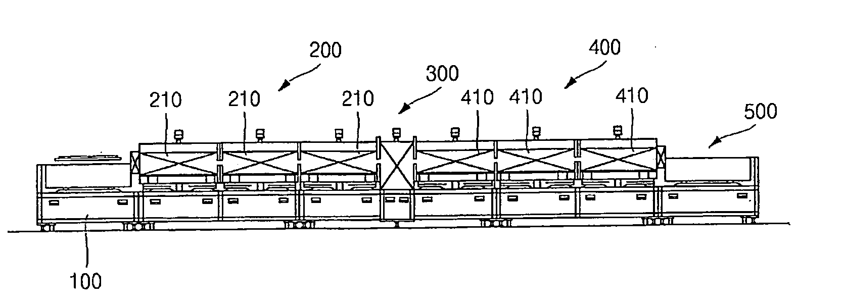
[0036] The heat treatment system for the semiconductor device according to the present invention can rapidly perform the heat treatment process for the semiconductor device by gradually increasing the temperature of the semiconductor device. In particular, the heat treatment system of the present invention can rapidly perform the heat treatment process, such as the crystallization process for the amorphous silicon thin film formed on the upper surface of the glass substrate, the dopant activation process for the TFT device consisting of the poly-crystalline silicon thin film, or the pre-compaction process for the glass substrate to form the silicon thin film on the upper surface of the glass substrate, while preventing the semiconductor device from being deformed. In addition, the heat treatment system of the present invention uniformly heats the semiconductor device while supporting the semiconductor device using the support plate, so the glass substrate can be prevented from being deformed or damaged.
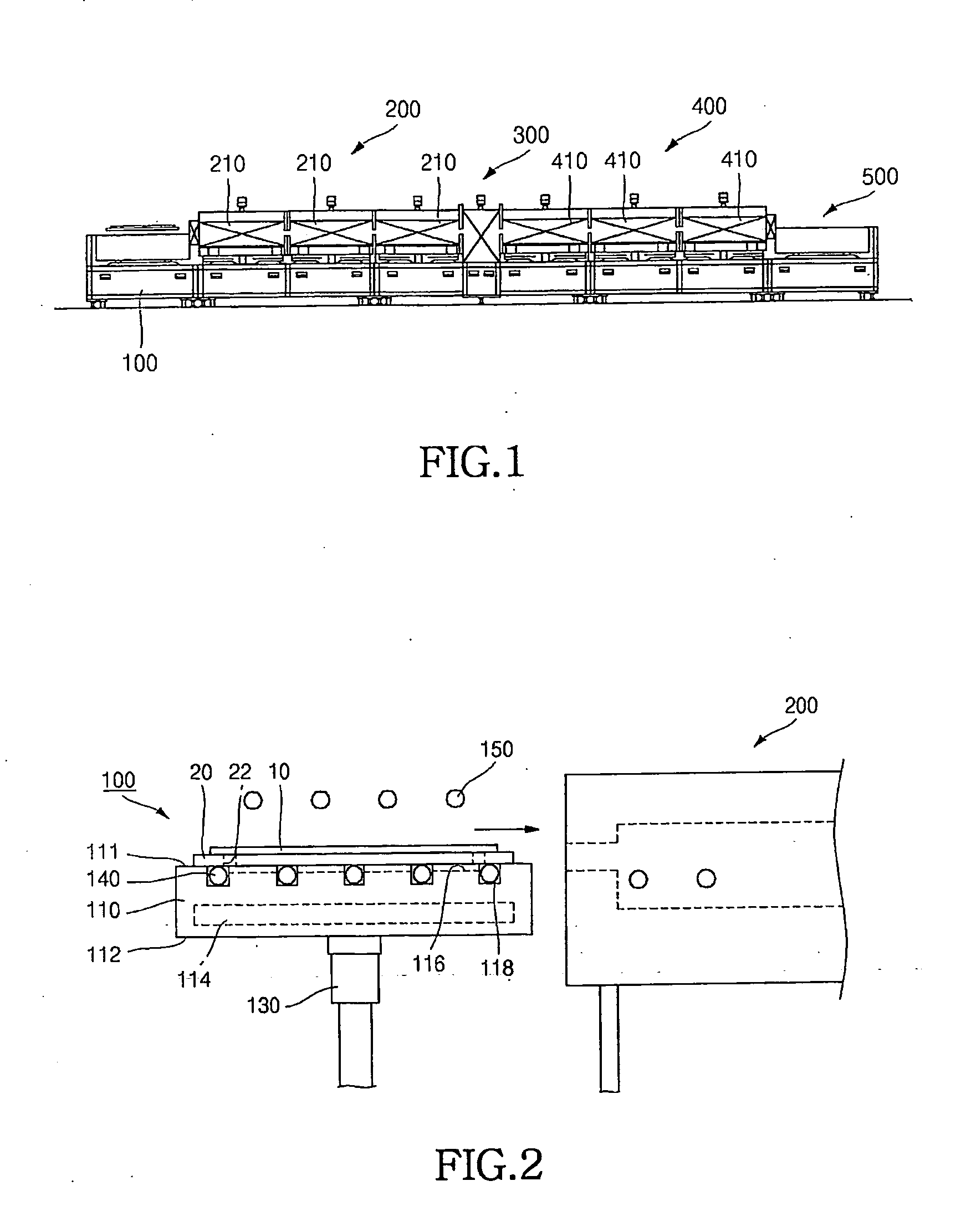
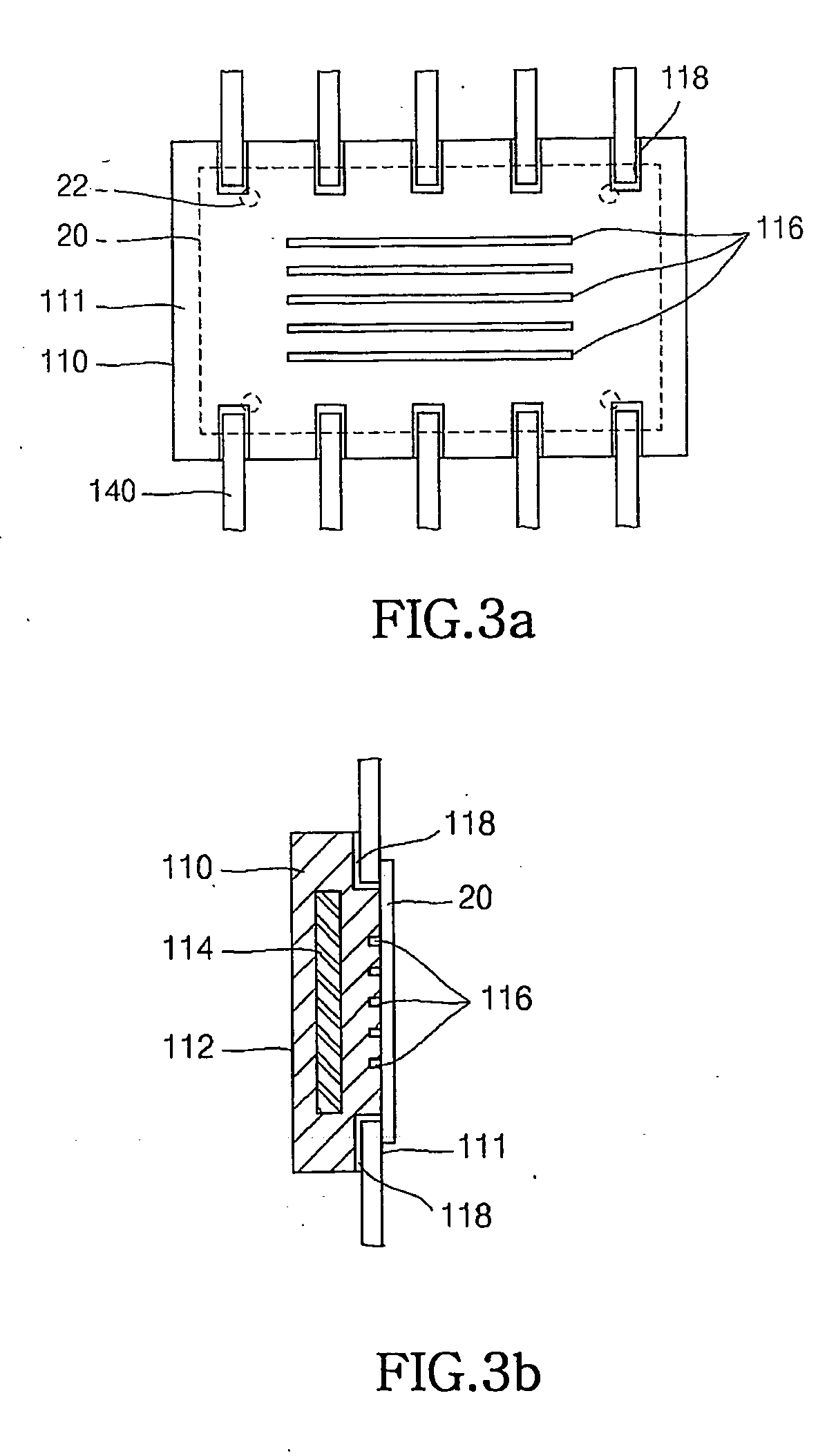
[0037] According to the present invention, a contact area between the semiconductor device and the susceptor is relatively small in the center portion thereof so an amount of heat transferred to the center portion of the semiconductor device is less than an amount of heat transferred to the outer peripheral portion of the semiconductor device. Thus, the semiconductor device can be uniformly preheated over the whole area thereof so that deformation of the semiconductor device caused by the local temperature difference in the semiconductor device can be prevented.
[0038] In addition, according to the present invention, the processing unit applies heat to the semiconductor device by using heat generated from the lamp heater and induction heating derived from induced electromotive force, so that the heat treatment process for the semiconductor device can be performed under the higher temperature atmosphere while preventing the semiconductor device from being deformed.
[0039] According to the present invention, the unloading unit sprays cooling gas onto the semiconductor device being conveyed, thereby uniformly cooling the semiconductor device. Thus, heat treatment process for the semiconductor device can be rapidly performed while preventing the semiconductor device from being deformed or damaged.
[0040] In addition, according to the present invention, the unloading unit applies heat to the upper portion of the semiconductor device by means of a heating device while spraying gas onto the lower surface of the support plate supporting the semiconductor device, so that the semiconductor device and the support plate can be uniformly cooled while preventing the deformation of the semiconductor device caused by the local temperature difference in the semiconductor device.

Problems solved by technology

However, if the heat treatment temperature is too low, a grain size may be reduced and crystallinity thereof may be degraded, thereby lowering driving characteristics of the semiconductor device.
In particular, if the added metal element is introduced into a channel area of a transistor, current leakage may be increased.
Although the ELC process can crystallize the amorphous silicon thin film without deforming the glass substrate, a line pattern bonding may be created due to the high-energy laser or an uneven crystalline phase may occur if high-energy laser is unevenly irradiated onto the amorphous silicon thin film, thereby lowering driving characteristics of the semiconductor device.
In addition, the ELC process requires expensive equipment, so the ELC process increases the initial investment cost while presenting limitations to produce the semiconductor devices in mass production.
Thus, the ELA process also has the problems represented in the ELC process.
That is, the ELA process may cause thermal stress to the poly-crystalline silicon thin film if the amorphous silicon thin film is unevenly crystallized or melted due to high-energy laser unevenly irradiated onto the amorphous silicon thin film, thereby degrading reliability of the semiconductor device.
However, the RTA process may cause deformation of the glass substrate if the heat treatment process is continuously performed more than several minutes at the temperature above 600° C. In contrast, if the heat treatment process is performed at the temperature below 600° C., the dopant cannot be sufficiently activated, thereby degrading the characteristics of the semiconductor devices.
However, the FA process cannot sufficiently activate the dopant if the heat treatment temperature is lowered, thereby degrading reliability of the semiconductor devices.
In addition, since the FA process requires several hours of process time, productivity thereof may be lowered.
When the above crystallization processes or the dopant activation processes for the amorphous silicon thin film are carried out, the heat treatment temperature may exert a serious influence upon process time, quality of the poly-crystalline silicon thin film, and reliability of the semiconductor devices.
If a local temperature deviation occurs in the glass substrate, the glass substrate may be seriously deformed or damaged.
Thus, the glass substrate is subject to thermal stress due to the temperature difference, so that the glass substrate is easily deformed.
In addition, even when the glass substrate is maintained in a constant temperature, if the glass substrate has an uneven temperature distribution, the glass substrate is deformed due to thermal stress or the glass substrate is unevenly shrunk due to the densification behavior, causing deformation of the glass substrate.
Due to the long process time for the heat treatment process, the horizontal continuous furnace may not significantly increase the heat treatment temperature to avoid the deformation of the glass substrate.
In particular, in cases of large-sized glass substrates, there is a great difference of heating and cooling speeds between the outer portions and the inner portions of the glass substrates, so that the glass substrates may be seriously deformed.
In addition, contact portions of the glass substrates, which make contact with the boat, may represent the heating and cooling speeds different from those of non-contact portions of the glass substrates, which do not make contact with the boat, so that the glass substrate is unevenly heated or cooled.
Therefore, the vertical tube furnace must slowly heat or cool the glass substrates (for example, it heats or cools five glass substrates per one minute) in order to reduce the difference of the heating and cooling speeds between the inner and outer portions of the glass substrates, so relatively long process time is required.
In addition, since the glass substrates are installed in the vertical tube furnace while being supported by the boat, if the heat treatment process is performed for a long period of time at the temperature above 500° C., the glass substrates may droop due to the tare thereof, so the vertical tube furnace is not applicable for the dopant activation process or the SPC process, which are performed at the temperature above 600° C., but only applicable for the heat treatment process performed at the temperature below 500° C.

Method used


Image

  • System for heat treatment of semiconductor device
  • System for heat treatment of semiconductor device
  • System for heat treatment of semiconductor device

Examples


application example 1

[0161] According to application example 1, the heat treatment system of the present invention is used for the SPC process of the amorphous silicon thin film deposited on the semiconductor device, that is, the glass substrate.

[0162]FIG. 17 is a graph illustrating a UV slope, which represents the crystallization degree of the amorphous silicon thin film as a function of current of the induction coil. That is, FIG. 17 shows the crystallization degree of the amorphous silicon thin film as a function of current of the induction coil under the same heat treatment time for the glass substrate, wherein an X-axis represents the current of the induction coil and a Y-axis represents the UV curve. The crystallization degree of the amorphous silicon thin film according to a UV transmittance spectrum may be estimated based on the UV slope value, wherein a silicon thin film having high quality crystalline can be obtained as the UV slope value becomes high.

[0163]FIGS. 18a to 18d are graphs illust...

application example 2

[0166] According to application example 2, the heat treatment system of the present invention is used for the MILC process of the amorphous silicon thin film deposited on the semiconductor device, that is, the glass substrate.

[0167]FIG. 19 is a view illustrating a growing length of an MILC layer as a function of current of the induction coil after the MICL process has been finished.

[0168] After depositing the amorphous silicon thin film on the glass substrate through the chemical vapor deposition process, a metal element (Ni) is coated on a predetermined portion of the amorphous silicon thin film in order to perform the MILC process. Herein, the MILC process is performed in the same manner as the crystallization process of application example 1, except that the preheating temperature of the furnace is set to 600° C., which is lower than that of application example 1. At this time, the processing unit 300 performs the heat treatment process while adjusting current applied to the ha...

application example 3

[0170] According to application example 3, the heat treatment system of the present invention is used for the dopant activation process to activate the dopant doped into the crystalline silicon thin film.

[0171]FIG. 20 is a graph illustrating the activation degree of the dopant as a function of the heating temperature and power of halogen lamps.

[0172] After depositing the amorphous silicon thin film on the glass substrate through the chemical vapor deposition process, the amorphous silicon thin film is crystallized into the poly-crystalline silicon thin film through the ELC process. Then, after depositing a silicon dioxide (SiO2) layer as an insulation layer, an n-type dopant is doped into the poly-crystalline silicon thin film by using doping equipment. According to application example 3, the dopant activation process is performed in the same manner as the crystallization process and the MILC process used in application examples 1 and 2, except that the preheating temperature of t...


PUM

PropertyMeasurementUnit
Temperatureaaaaaaaaaa
Lengthaaaaaaaaaa
Fractionaaaaaaaaaa

Abstract

Disclosed is a heat treatment system for semiconductor devices. The heat treatment system is used in a heat treatment process for semiconductor devices, such as a crystallization process for an amorphous silicon thin film or a dopant activation process for a poly-crystalline silicon thin film formed on a surface of a glass substrate of a flat display panel including a liquid crystal display (LCD) or an organic light emitting device (OLED). The heat treatment system transfers a semiconductor device after uniformly preheating the semiconductor device in order to prevent deformation of the semiconductor device during the heat treatment process, rapidly performs the heat treatment process under the high temperature condition by heating the semiconductor device using a lamp heater and induction heat derived from induced electromotive force, and unloads the semiconductor device after uniformly cooling the semiconductor device such that the semiconductor device is prevented from being deformed when the heat treatment process has been finished. The heat treatment system rapidly performs the heat treatment process while preventing deformation of the semiconductor device by gradually heating or cooling the semiconductor device.

Description

TECHNICAL FIELD [0001] The present invention relates to a heat treatment system for semiconductor devices. More particularly, the present invention relates to a heat treatment system for semiconductor devices used in a heat treatment process, such as a crystallization process for an amorphous silicon thin film or a dopant activation process for a poly-crystalline silicon thin film formed on a surface of a glass substrate of a flat display panel including a liquid crystal display (LCD) or an organic light emitting device (OLED), wherein the heat treatment system according to the present invention transfers a semiconductor device after uniformly preheating the semiconductor device in order to prevent deformation of the semiconductor device during the heat treatment process, rapidly performs the heat treatment process under the high temperature condition by heating the semiconductor device using a lamp heater and induction heat derived from induced electromotive force, and unloads the ...

Claims


Application Information

Patent Timeline
IPC IPC(8): H01L21/00H01L21/82H01L21/324
CPCH01L21/67109H01L21/67115H01L21/67173H01L21/67207H01L21/67236
Inventor PARK, WANG JUNKIM, JUNG BAEAHN, YOUNG JAEKIMSHIN, DONG HOON
Owner VIATRON TECH INC
Learn More