Reconfigurable switched- capacitor input circuit with digital-stimulus acceptability for analog tests
- Summary
- Abstract
- Description
- Claims
- Application Information
AI Technical Summary
Benefits of technology
Problems solved by technology
Method used
Image
Examples
first embodiment
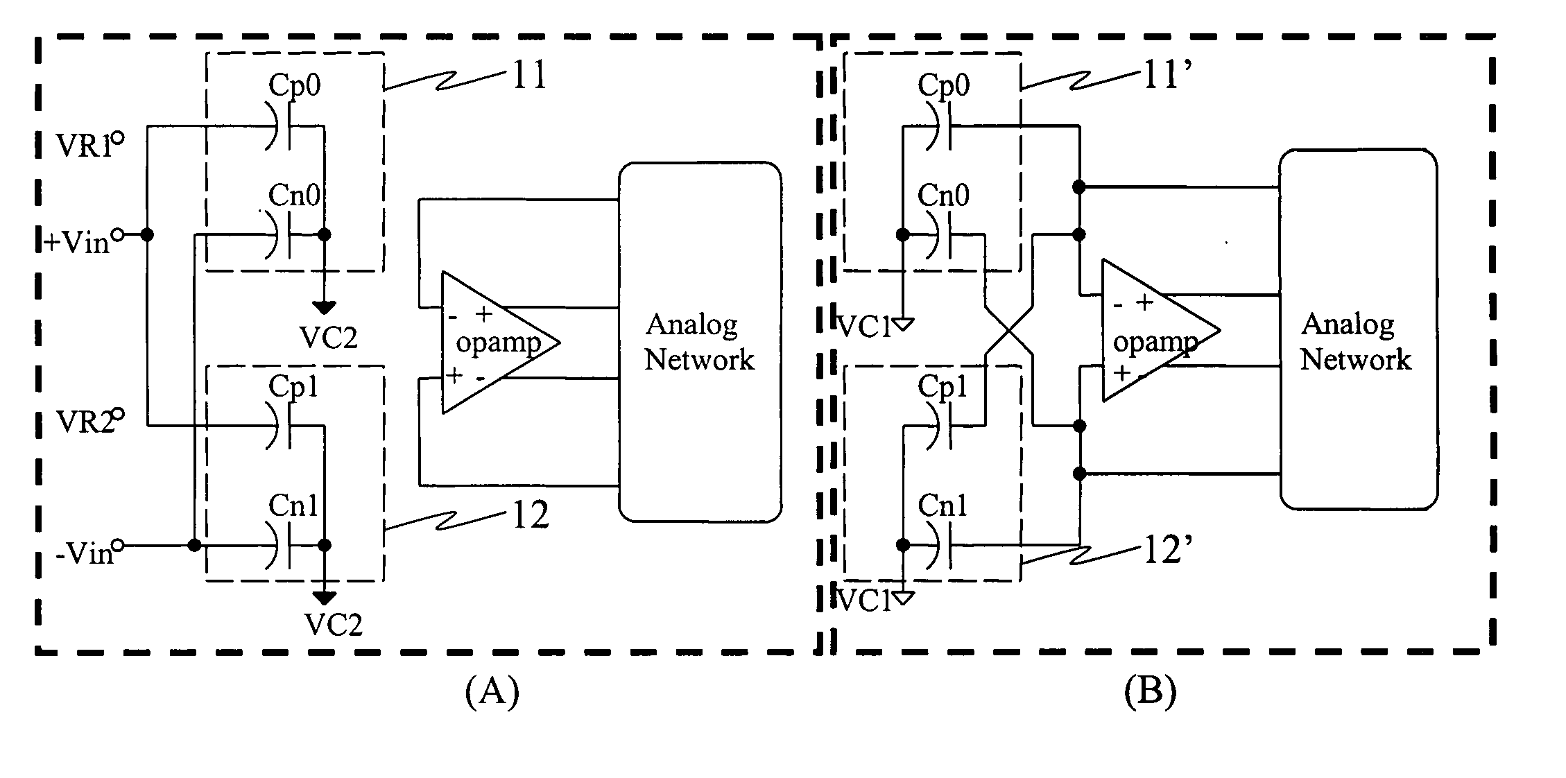
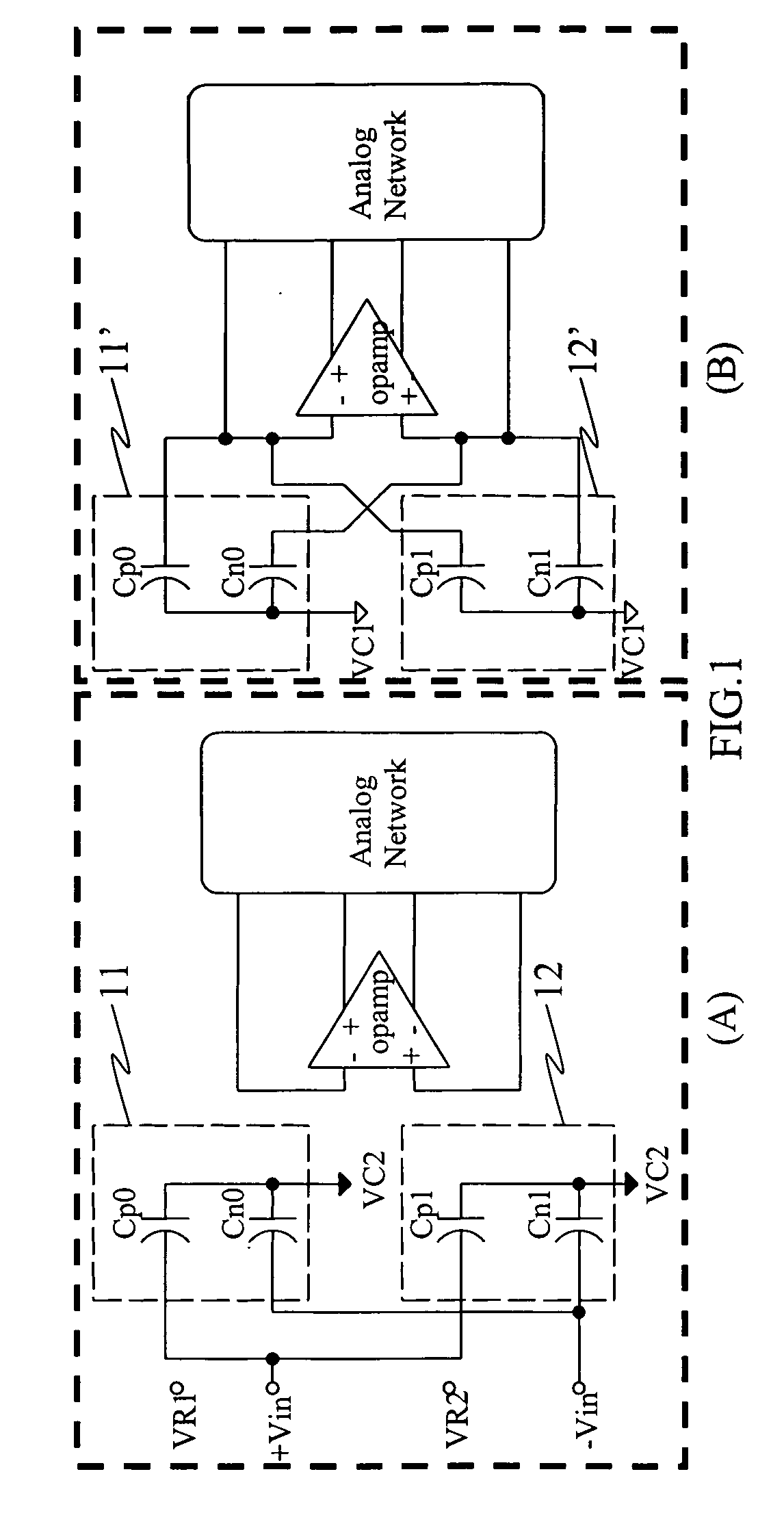
[0036] To better understand the operation of the reconfigurable switched-capacitor input circuit, the circuit connections in the two non-overlapped clock phases are described. FIG. 1 represents the operation of the reconfigurable switched-capacitor input circuit in the normal mode for the present invention that exerts at least two switched-capacitor sets. FIG. 1(A) shows the circuit connections in the first clock phase. The digital switching-signal generator generates the switching signals to control the analog-signal switches of the switched-capacitor sets 11 and 12 so that the bottom ends of the first capacitors Cp0 and Cp1 of the switched-capacitor sets connect to the analog input positive phase voltage signal +Vin and the bottom ends of the second capacitors Cn0 and Cn1 of the switched-capacitor sets connect to the analog input negative phase voltage signal −Vin. And all the top ends of the capacitors Cp0, Cn0, Cp1 and Cn1 connect to the direct current voltage source VC2. The ci...
second embodiment
[0040] Actually, the operation of the input circuit of the circuit under test in the normal mode is not limited by that revealed in FIG. 1. The second embodiment with regard to the reconfigurable switched-capacitor input circuit in the normal mode is introduced in FIG. 3, wherein FIG. 3(A) and FIG. 3(B) represent the circuit connections in the two non-overlapped clock phases respectively. The circuit connections of the input circuit in the first clock phase are provided in FIG. 3(A). The digital switching-signal generator generates the switching signals to connect the analog input positive phase voltage signal +Vin to the bottom ends of the first capacitors Cp0 and Cp1 of the switched-capacitor sets 31 and 32 and, in the meantime, to connect the analog input negative phase voltage signal −Vin to the bottom ends of the second capacitors Cn0 and Cn1 of the switched-capacitor sets 31 and 32. The top ends of the first capacitors of the switched-capacitor sets are connected to the negati...
third embodiment
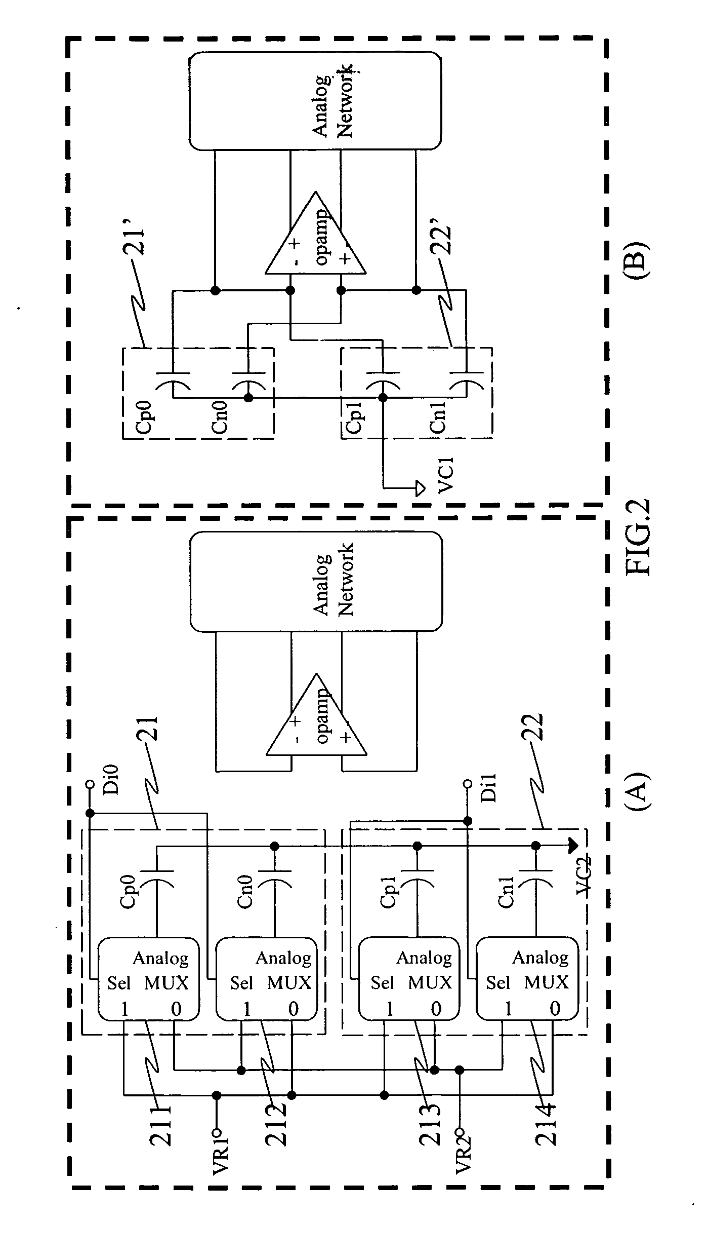
[0042] Additionally, the test mode operation of this invention whose normal mode operation is described in FIG. 1 is unfolded in FIG. 4. Similar to the disclosure in FIG. 2, the circuit connections in the two non-overlapped clock phases in the test mode are shown in FIG. 4(A) and FIG. 4(B) respectively. In the first clock phase, the digital switching-signal generator generates the switching signals to control the analog-signal switches of the switched-capacitor sets 41 and 42 to make the top ends of the capacitors Cp0, Cn0, Cp1 and Cn1 inside the switched-capacitor sets 41 and 42 connecting to the direct current voltage source VC2 as illustrated in FIG. 4(A). At the same time, the bottom ends of the first capacitors Cp0 and Cp1 and the second capacitors Cn0 and Cn1 inside the switched-capacitor sets 41 and 42 are connected to the direct current voltage source VR1 and the direct current voltage source VR2 respectively. One part of what illustrated in FIG. 4(B) is that all the bottom ...
PUM
 Abstract
Description
Claims
Application Information
 - R&D
- Intellectual Property
- Life Sciences
- Materials
- Tech Scout
- Unparalleled Data Quality
- Higher Quality Content
- 60% Fewer Hallucinations
Browse by: Latest US Patents, China's latest patents, Technical Efficacy Thesaurus, Application Domain, Technology Topic, Popular Technical Reports.
© 2025 PatSnap. All rights reserved.Legal|Privacy policy|Modern Slavery Act Transparency Statement|Sitemap|About US| Contact US: help@patsnap.com


