Heterojunction bipolar transistor

a bipolar transistor and heterojunction technology, applied in the field of heterojunction bipolar transistors, can solve the problems of inp/gaassb/inp-based hbt still having unsolved problems, subsequent increase of emitter junction capacitance, excess electron accumulation, etc., to reduce or reverse the current gain drop, increase the operating speed, and reduce the effect of emitter/base

Inactive Publication Date: 2006-10-19
NIPPON TELEGRAPH & TELEPHONE CORP
View PDF2 Cites 0 Cited by
  • Summary
  • Abstract
  • Description
  • Claims
  • Application Information

AI Technical Summary

Benefits of technology

[0016] In the present invention as explained above, in a heterostructure bipolar transistor having a GaAsSb-based material as a base layer, an emitter layer is made of a compound semiconductor containing indium, aluminum, and phosphorus, so the emitter / base ΔEc can be reduced or reversed. This achieves a remarkable effect of allowing a heterostructure bipolar transistor using GaAsSb as a base to suppress the current gain drop and increase the operating speed, by, e.g., reducing the base-emitter capacitance and increasing the current gain, without decreasing the resistance of GaAsSb against hydrogen passivation and the reliability of a device.

Problems solved by technology

Problems to be Solved by the Invention Unfortunately, the InP / GaAsSb / InP-based HBT still has unsolved problems.
One problem is the excess accumulation of emitter injection electrons caused by the discontinuity of the emitter / base conduction band edge, and the subsequent increase in emitter junction capacitance.
This band discontinuity may cause excess electron accumulation in an emitter space-charge region.
In addition, if a forward voltage is increased to supply a high electric current, a local potential drop occurs in the conduction band edge near the emitter / base interface, and this further increases the electron accumulation.
Any of these problems functions as a capacitive component with respect to a device operation, and interferes with a high-speed operation of the device.
These problems also increase a tunneling recombination current via a defect level near the emitter / base interface, thereby lowering the current gain.

Method used


Image

  • Heterojunction bipolar transistor
  • Heterojunction bipolar transistor
  • Heterojunction bipolar transistor

Examples


Embodiment Construction

[0034] Embodiments of the present invention will be described below with reference to the accompanying drawings.

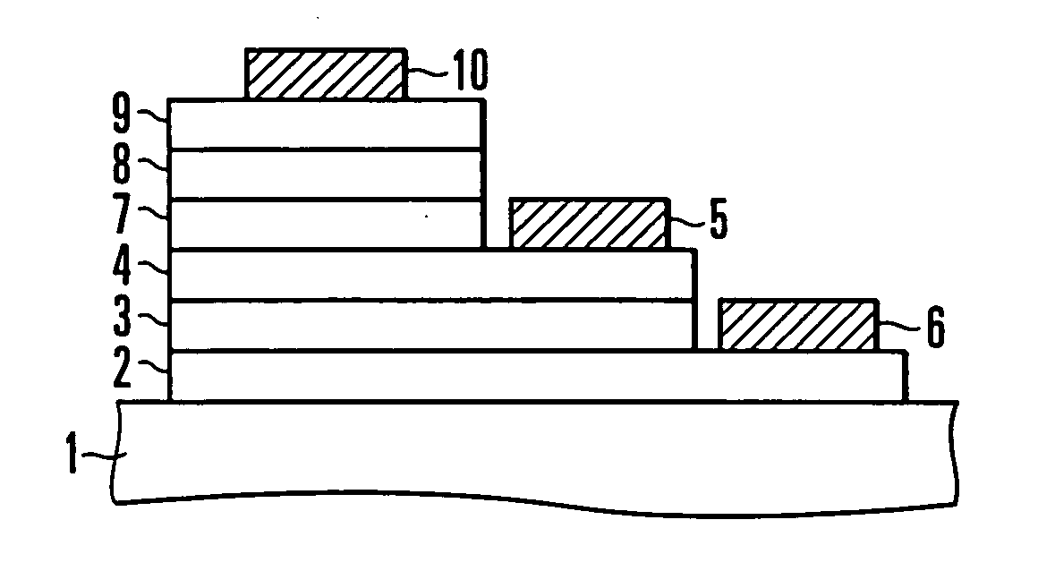
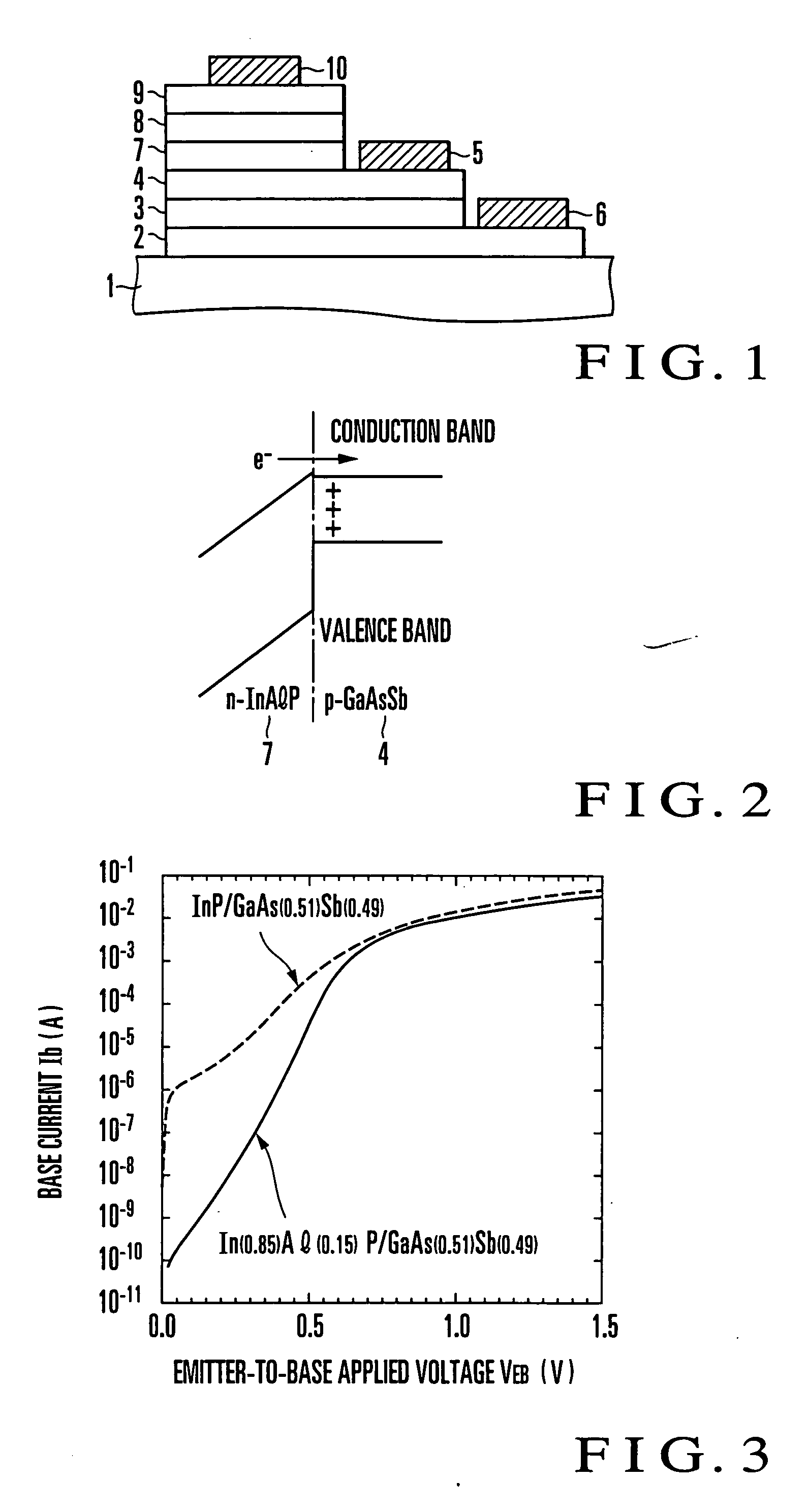
[0035]FIG. 1 is a schematic sectional view showing an example of the arrangement of a heterostructure bipolar transistor according to an embodiment of the present invention. In this heterostructure bipolar transistor shown in FIG. 1, an n-type InP sub collector layer 2 heavily doped with silicon (Si), an InP collector layer 3, a p-type GaAs(0.51)Sb(0.49) base layer 4 heavily doped with carbon (C), an n-type In(1-y)Al(y)P emitter layer 7 doped with Si, an n-type InP cap layer 8 heavily doped with Si, and an n-type In(0.53)Ga(0.47)As contact layer 9 heavily doped with Si are stacked on an InP substrate 1 having a resistance increased by doping iron (Fe) as an impurity and having a (100) major surface.

[0036] In addition, an ohmic-contact collector electrode 6 is formed on a region of the sub collector layer 2 where the collector layer 3 is not formed, an ohmic-contact base ...


PUM


Abstract

An n-type InP sub collector layer 2 heavily doped with silicon (Si), an InP collector layer 3, a p-type GaAs(0.51)Sb(0.49) base layer 4 heavily doped with carbon (C), an n-type In(1-y)Al(y)P emitter layer 7 doped with Si, an n-type InP cap layer 8 heavily doped with Si, and an n-type In(0.53)Ga(0.47)As contact layer 9 heavily doped with Si are stacked on a substrate 1.

Description

TECHNICAL FIELD [0001] The present invention relates to a heterostructure bipolar transistor having a base made of GaAsSb. BACKGROUND ART [0002] GaAsSb is attracting attention as a compound semiconductor used as a base layer material of an InP-based heterostructure bipolar transistor (HBT). GaAsSb lattice-matches an InP substrate by a composition GaAs(0.51)Sb(0.49). An InP / GaAs(0.51)Sb(0.49) / InP-based HBT using GaAsSb as a base can realize good high-frequency characteristics and high-breakdown-voltage characteristics at the same time (reference 1: “300 GHz InP / GaAsSb / InP Double HBTs with High Current Capability and BVceo≧6 V”, M. W. Dvorak, Student Member, IEEE, C. R. Bolognesi, Member, IEEE, O. J. Pitts, and S. P. Watkins, Member, IEEE,: IEEE ELECTRON DEVICE LETTERS, VOL. 22, NO. 8, AUGUST 2001 p. 361). Heterostructures include a type-I heterostructure in which a conduction band ECA and valence band EVA of a semiconductor A and a conduction band ECB and valence band EVB of a semico...

Claims


Application Information

Patent Timeline
IPC IPC(8): H01L29/732
CPCH01L29/0817H01L29/7371H01L29/205
Inventor ODA, YASUHIROKURISHIMA, KENJIYOKOYAMA, HARUKIKOBAYASHI, TAKASHI
Owner NIPPON TELEGRAPH & TELEPHONE CORP
Why Eureka
Try Eureka