Optical semiconductor element, method of manufacturing optical semiconductor element and optical module
a manufacturing method and semiconductor technology, applied in semiconductor lasers, laser optical resonator construction, laser details, etc., can solve the problems of degrading laser characteristics, poor depth direction control, wet etching, etc., to achieve stable optical output power, slope efficiency, and high solid solubility
- Summary
- Abstract
- Description
- Claims
- Application Information
AI Technical Summary
Benefits of technology
Problems solved by technology
Method used
Image

Examples
example 1
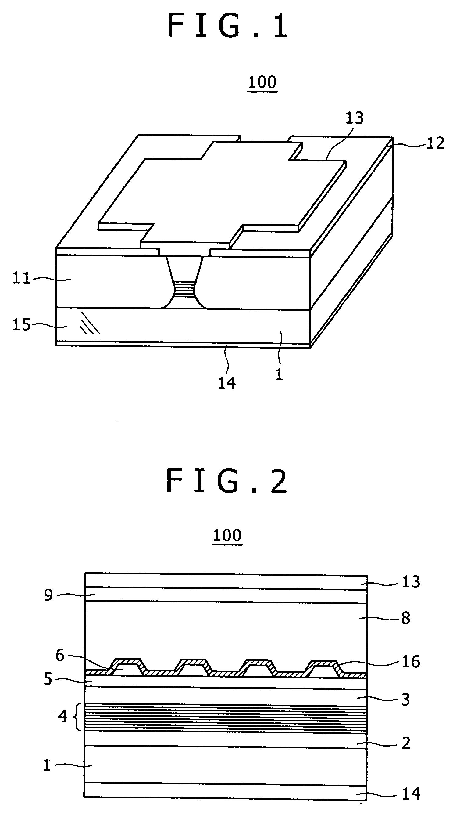
[0017] Referring to FIGS. 1 and 2, Example 1 of an optical semiconductor element will be discussed below. FIG. 1 is a perspective view showing a buried heterostructure semiconductor laser including a floating diffraction grating. FIG. 2 is a sectional view taken along a waveguide of FIG. 1.
[0018] Referring to FIGS. 1 and 2, the following will describe the manufacturing process of an optical semiconductor element 100. First, a multilayer structure is formed on an InP substrate 1 by metal-organic chemical vapor deposition (MOCVD). In the multilayer structure, a lower guide layer 2, an InGaAsP multiple quantum well active layer 4, an InGaAsP upper guide layer 3, an InP etching stop layer 5, an InGaAsP layer 6 serving as a diffraction grating, and an InP cap layer (not shown) serving as the protection layer of the InGaAsP layer 6 are formed in this order. After the InP cap layer is removed, a photo resist is coated and a photo resist pattern with a period of about 200 nm is formed on t...
example 2
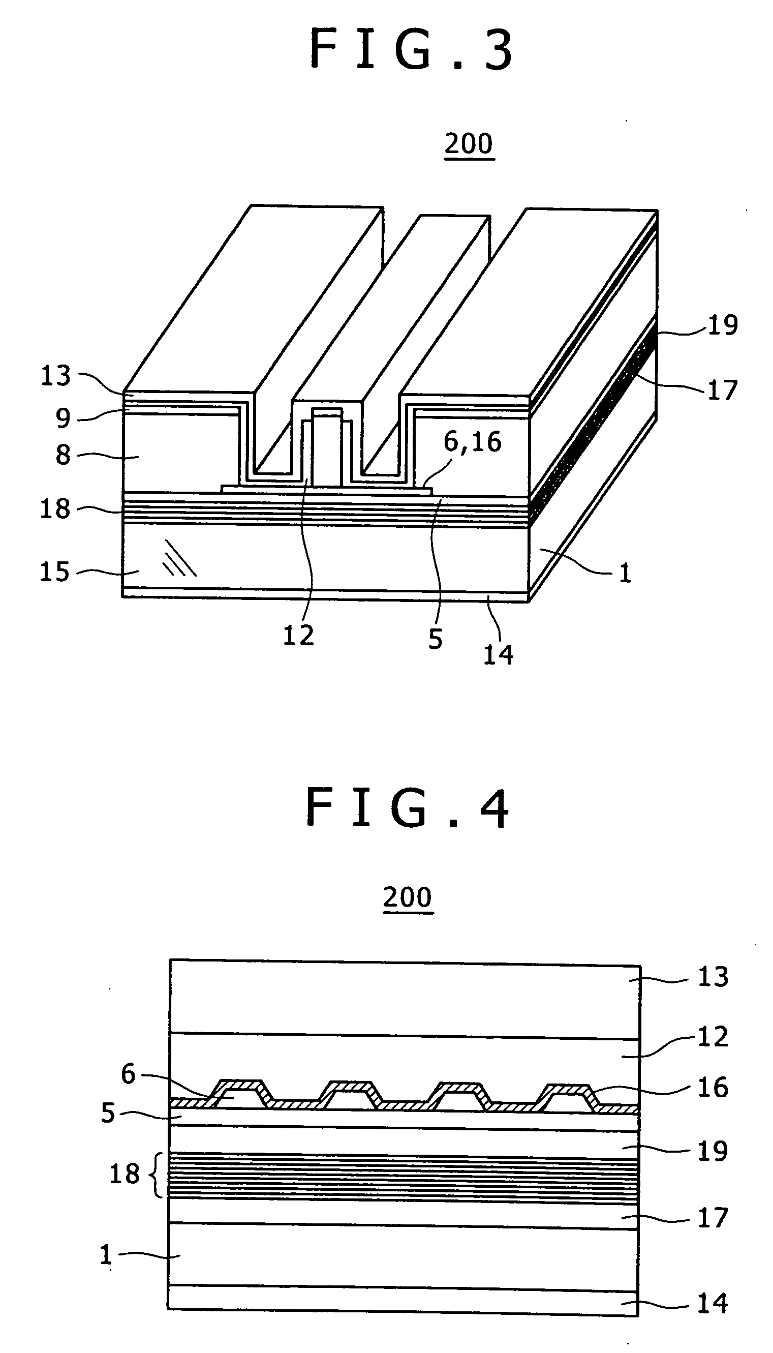
[0029] Referring to FIGS. 3 and 4, Example 2 of an optical semiconductor element will be discussed below. FIG. 3 is a perspective view showing a ridge waveguide semiconductor laser including a floating diffraction grating. FIG. 4 is a sectional view taken along a groove beside a waveguide of FIG. 3.
[0030] Referring to FIGS. 3 and 4, the following will describe the manufacturing process of an optical semiconductor element 200. First, to form an optical waveguide, a multilayer structure is formed on an InP substrate 1 by metal-organic chemical vapor deposition (MOCVD). In the multilayer structure, an n-type InAlAs layer 17, an InGaAlAs multiple quantum well active layer 18, a p-type InAlAs layer 19, an InP etching stop layer 5, an InGaAsP layer 6 serving as a diffraction grating layer, and an InP cap layer (not shown) serving as the protection layer of the InGaAsP layer 6 are formed in this order. Then, the InP cap layer is removed. After a photo resist is coated, a photo resist patt...
example 3
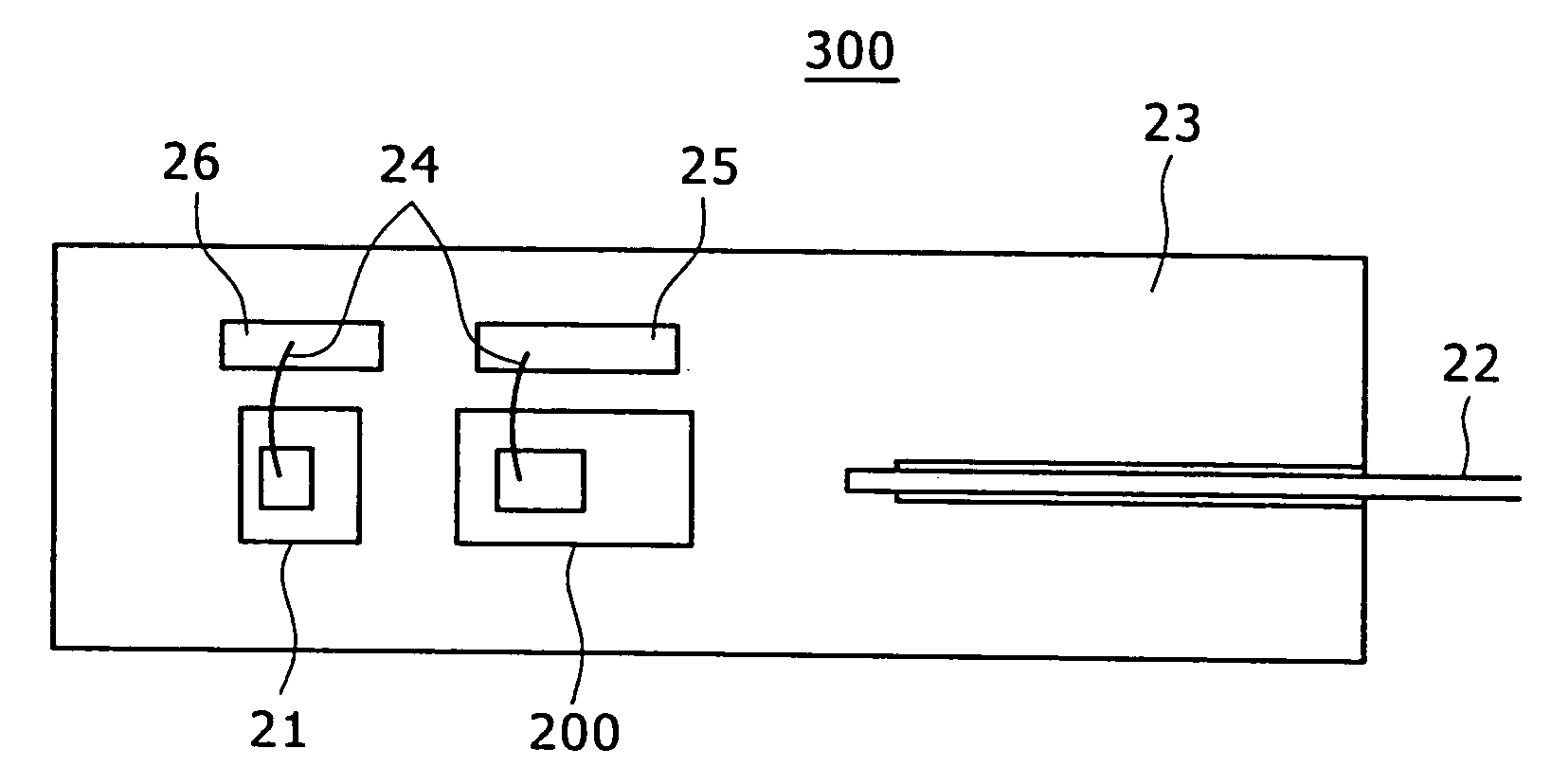
[0041] Referring to FIG. 5, Example 3 of an optical module will be discussed below. FIG. 5 is a block diagram for explaining the configuration of the optical module.
[0042] In FIG. 5, an optical module 300 has an optical fiber 22 mounted in the groove of a silicon substrate 23 and a semiconductor laser 200 mounted on the silicon substrate 23. The semiconductor laser 200 is aligned with the optical fiber 22. A waveguide light-receiving element 21 is mounted on the silicon substrate 23 so as to monitor light in the rear of the semiconductor laser. The semiconductor laser 200 and the waveguide light-receiving element 21 are respectively connected to terminals 25 and 26, which are mounted on the silicon substrate 23, via bonding wires 24. The terminals 25 and 26 are connected to external terminals (not shown).
[0043] The optical module 300 includes a housing (not shown). The input terminal of the optical fiber and optical components mounted on the silicon substrate 23 are housed in the ...
PUM
 Abstract
Description
Claims
Application Information
 - R&D
- Intellectual Property
- Life Sciences
- Materials
- Tech Scout
- Unparalleled Data Quality
- Higher Quality Content
- 60% Fewer Hallucinations
Browse by: Latest US Patents, China's latest patents, Technical Efficacy Thesaurus, Application Domain, Technology Topic, Popular Technical Reports.
© 2025 PatSnap. All rights reserved.Legal|Privacy policy|Modern Slavery Act Transparency Statement|Sitemap|About US| Contact US: help@patsnap.com