Ferroelectric material, its manufacture method and ferroelectric memory
- Summary
- Abstract
- Description
- Claims
- Application Information
AI Technical Summary
Benefits of technology
Problems solved by technology
Method used
Image
Examples
Embodiment Construction
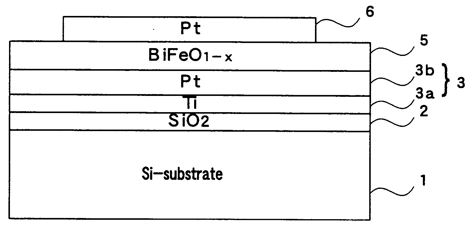
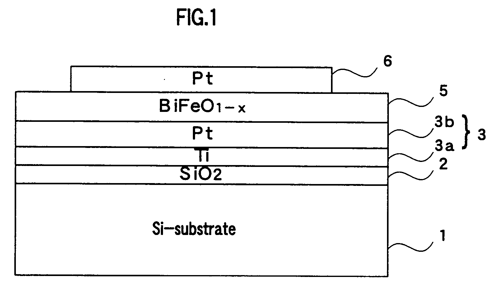
[0028]FIG. 1 is a cross sectional view of a capacitor made of ferroelectric material according to an embodiment. On the surface of a substrate 1 made of n-type silicon, a silicon oxide film 2 is formed. For example, the silicon oxide film 2 is formed by thermal oxidation. A lower electrode film 3, a capacitor dielectric film 5 and an upper electrode film 6 are formed in this order on the silicon oxide film 2. The lower electrode film 3 has a two-layer structure of a Ti film 3a having a thickness of 60 nm and a Pt film 3b having a thickness of 100 nm. For example, the Ti film 3a and Pt film 3b can be formed by sputtering.
[0029] The capacitor dielectric film 5 is formed, for example, by chemical solution deposition (CSD). This film forming procedure will be described in the following. Precursor solution of BiFeO3 is spin-coated on the lower electrode 3. For example, solvent for this precursor solution is 2-methoxyethanol, and the concentration of BiFeO3 is 0.15 mol %. The substrate i...
PUM
| Property | Measurement | Unit |
|---|---|---|
| Temperature | aaaaa | aaaaa |
| Temperature | aaaaa | aaaaa |
| Lattice constant | aaaaa | aaaaa |
Abstract
Description
Claims
Application Information
 - R&D
- Intellectual Property
- Life Sciences
- Materials
- Tech Scout
- Unparalleled Data Quality
- Higher Quality Content
- 60% Fewer Hallucinations
Browse by: Latest US Patents, China's latest patents, Technical Efficacy Thesaurus, Application Domain, Technology Topic, Popular Technical Reports.
© 2025 PatSnap. All rights reserved.Legal|Privacy policy|Modern Slavery Act Transparency Statement|Sitemap|About US| Contact US: help@patsnap.com


