
Semiconductor device and method of fabricating a semiconductor device

Inactive Publication Date: 2006-05-11
SEMEQUIP
View PDF17 Cites 17 Cited by
  • Summary
  • Abstract
  • Description
  • Claims
  • Application Information

AI Technical Summary

Benefits of technology

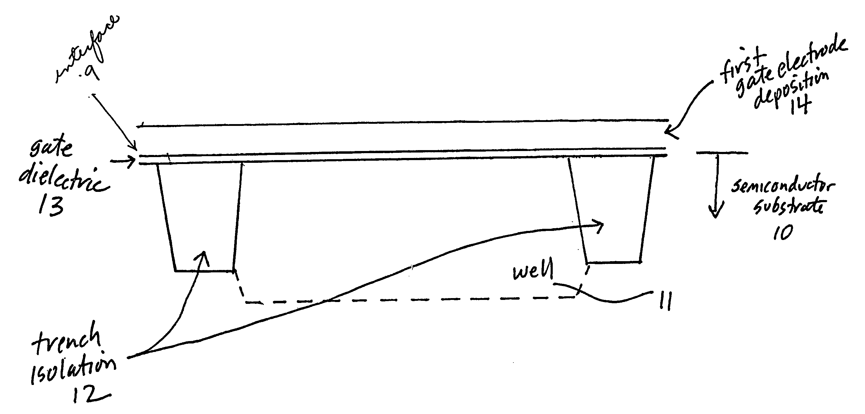
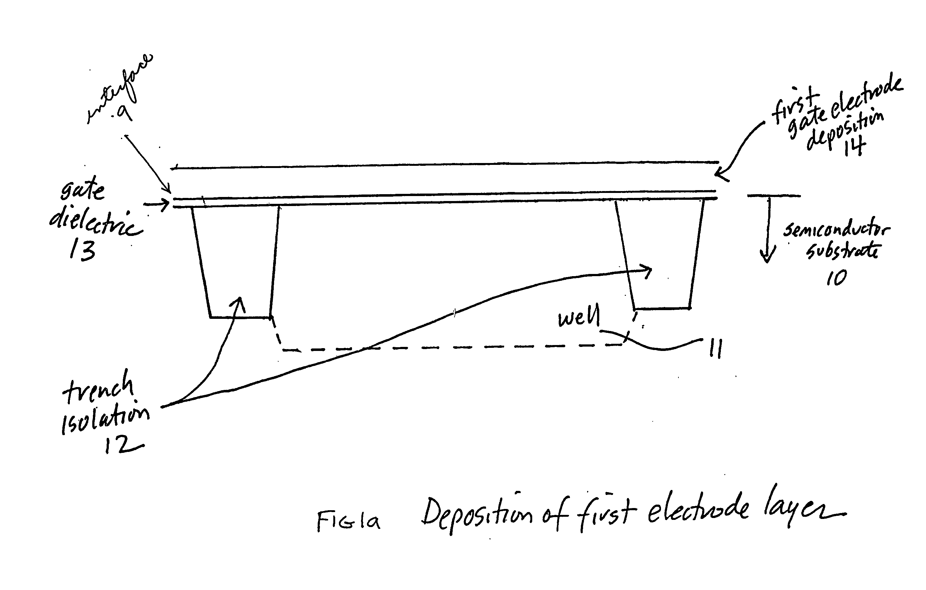
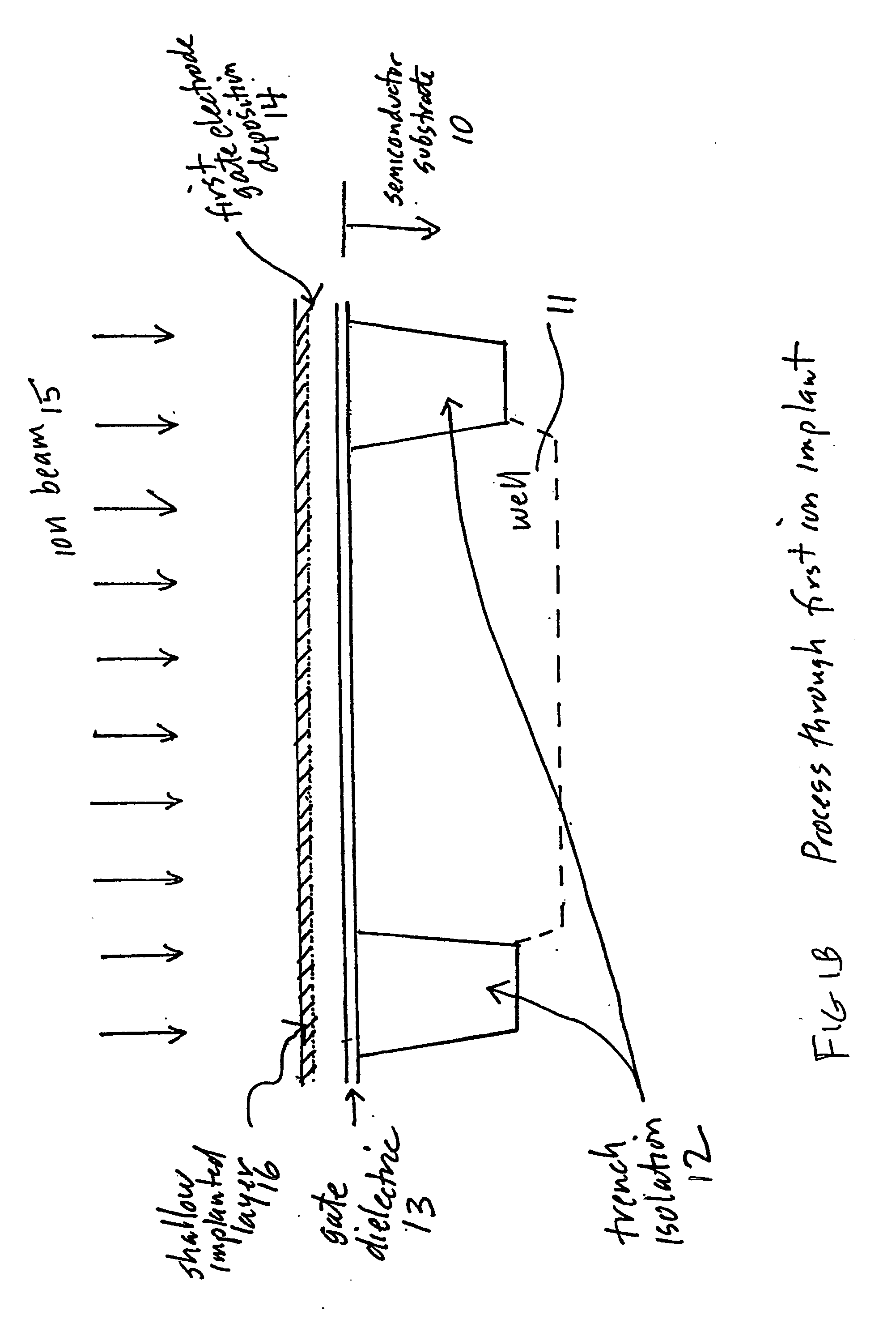
[0016] The present invention uses a two-deposition gate formation process to allow alternative process conditions, which address the issues of gate depletion and dopant penetration of the gate dielectric observed in conventional technologies. In particular, the present invention relates to the formation of a gate electrode by a combination of two-deposition-plus-implant sequences. The first deposition is thin and its corresponding implant is very shallow, to directly place a maximally effective dose as close to the gate electrode / gate dielectric interface as possible. The emergence of cluster ion implants which enable high dose, ultra low effective-energy implant processes, eliminates the previous constraints on doping very thin layers. The second deposition completes the gate electrode to a conventional thickness and allows the independent selection of the ion implant and heat treatments for the second deposition.
[0017] It may be noted that the advent of spike annealing further enables the formation of very shallow, highly activated dopant layers. A spike anneal is a rapid thermal process or heat treatment in which the time at the highest temperature approaches zero: the temperature is ramped up very quickly and immediately ramped down as quickly as possible. In the present invention, the formation of the shallow doped layer at the gate electrode / gate dielectric interface eliminates one of the constraints on the implant and heat treatment normally used for single gate processes: since there is no longer a need to diffuse the dopant through the gate electrode layer to the gate dielectric interface to combat gate depletion, a spike anneal can be used, further reducing the risk of dopant penetration of the gate dielectric.
[0018] Further benefits of this two-deposition gate formation process can be realized when two gate-patterning steps are included. In particular, one benefit of utilizing two patterning steps is that the drain extension implant can be used for both the first level gate doping step and the drain extension implant, eliminating one shallow implant from the process. Next, the use of two patterning steps allows the freedom to choose to offset the second pattern towards the source side of the gate. This would create an asymmetric source / drain transistor with much larger overlap of the drain extension region on the source side than the drain side. This is an effective means of creating the kind of transistor behavior described by Ghani, et al, while avoiding other layout and process constraints.
[0019] Another aspect of the invention relates to a method of fabricating an ultrashallow semiconductor junction by ion implantation of a dopant species into a dielectric layer on the surface of a semiconductor substrate and diffusing the dopant through the dielectric layer and into the semiconductor substrate, thereby creating a shallow semiconductor junction. The method is further comprised of implanting an additional species, or more than one additional species, where the action of the additional species is to enhance the diffusion of the dopant through the dielectric layer, thereby making the process more effective. One example of such a process is the implantation of a boron / hydrogen cluster ion into a silicon dioxide layer atop a silicon wafer. In this case, the hydrogen is known as set forth in the Fair reference, supra, to enhance the diffusion of boron in silicon dioxide, allowing management of the annealing process used to enable diffusion. This enhancement of the diffusion rate in oxide allows the relaxation of other process constraints, particularly on the time and temperature of the annealing treatment.

Problems solved by technology

There are various technical issues related to conventional CMOS processes as technology scaling progresses with regard to the doping of the gate electrode.
First, as the gate dielectric thickness is scaled down, the field intensity at the gate electrode / gate dielectric interface increases with the result that the gate electrode experiences depletion of charge starting at the dielectric interface.
This condition is undesirable because it has the effect of increasing the effective gate dielectric thickness, and modulating the threshold voltage.
Further, there is a competing issue that attempts to increase the doping of the gate electrode at the electrode / dielectric interface which enhances the risk of dopant diffusion through the gate dielectric and into the channel, particularly for boron doped gates.
Dopant penetration of the gate dielectric is undesirable because it changes the threshold voltage.
The grain boundary dopant at the gate electrode / gate dielectric interface is then a risk for gate dielectric penetration as the heat treatment continues.
This risk is increased as the heat treatment goes to higher temperatures and longer times. There are practical limits to the reduction of time / temperature for the gate electrode anneal, due to the need to diffuse the dopant to the gate electrode / gate dielectric interface and the need to electrically activate the implanted dopant, for example, as disclosed in M. Kase, et al.
The oxynitride gate dielectric is useful for the reduction of the boron penetration through the gate oxide, but does not help with the gate depletion effect.
The problem is that the SiGe gate material degrades the NMOS characteristics and thus requires complex selective technologies to achieve a full CMOS solution.
The metal gate approach solves the boron penetration problem (no boron to diffuse) and the gate depletion issue (near infinite charge concentration) but makes setting the threshold voltage for NMOS and PMOS simultaneously very difficult.
The metal gate approach also has significant challenges in process integration; since the metal layers are not physically stable at the high temperatures of the heat treatments required for implant activation, such as required by the source and drain regions.
The conventional device faces other limiting factors as technology scales.
With continued scaling, for example <0.1 um technology, the conventional device suffers from the need to provide sufficient gate overlap of the drain extension region to ensure high performance operation.
However, the process used by Ghani, et al in the demonstration devices is very constraining relative to large-scale production requirements: the structure requires a tilt implant selectively on the source side and not the drain side.
To manufacture devices with such a structure would require limiting the layout so that all sources are to one side and all drains to the other, making the circuit very large.
There are difficulties with continuing the historical methods of scaling the junction depth.
These implants have low productivity on a conventional implanter because they are in the regime where Child's Law applies; implants with energy of less than 10 keV.
While this method is able to increase productivity by around 2×, the deceleration beam has issues with energetic contamination and nonuniformity of implant results.
There are further issues with the conventional implant process for the formation of ultrashallow junctions in that the implant creates defect structures within the silicon implanted layer that pose more of an issue as the energy is reduced and the layer becomes shallower.
First, the density of created defects increases quickly because the implanted volume of the substrate material is reduced as the implant is made shallow.
Since the doses are either the same or increasing, the reduction of implant depth corresponds to an increase in both the density of implanted dopant and the implant defects.
As the defect density increases, the probability of interaction increases dramatically, with the problem that combinations of defects make more complex defect structures which are very difficult to anneal.
This is particularly an issue when the dopant concentration exceeds the solid solubility, since the supersaturated dopant tends to precipitate into undesirable structures.
For example, supersaturated boron tends to precipitate into silicon boride (SiB4), a structure which binds the boron into electrically inactive position, rendering that component of the boron implant completely ineffective.
The conventional process also places extreme constraints on the heat treatment, or anneal, used to make the implanted dopant electrically active.
There is a strong conflict between the need to heat the substrate to high temperatures to effectively activate the implanted dopant versus the need to limit the temperature and time of the anneal to prevent diffusion.
The method has the disadvantage, though, that diffusion through oxide is generally slower than through silicon, for example, as discussed in Fair, “Physical Models of Boron Diffusion in Ultrathin Gate Oxides”J. Electrochem. Soc, 144, 1997, p.
A further issue with the conventional process is the difficulty in avoiding implanting into an oxide while attempting to form an ultrashallow junction, for example, as discussed in Krull, et al, “The importance of the native oxide for sub-keV ion implants,”Proc.
As technology scales and the implant energy is reduced, it becomes increasingly difficult to remove the surface oxide well enough that it does not interfere with the ion implant process.

Method used


Image

  • Semiconductor device and method of fabricating a semiconductor device
  • Semiconductor device and method of fabricating a semiconductor device
  • Semiconductor device and method of fabricating a semiconductor device

Examples


Embodiment Construction

[0029] The present invention relates to a method for forming the gate electrode of an MOS transistor with a two-deposition process, as a means of addressing the issues of gate depletion and boron penetration of the gate dielectric, without requiring new materials. The present invention also relates to a method for forming an ultrashallow junction in a semiconductor substance.

Formation of Gate Electrode

[0030] As mentioned above, one aspect of the invention relates to the formation of a gate electrode of a MOS transistor by way of a two step deposition process. In the two-deposition process, the first step is the deposition of a thin layer of electrode material, followed by a shallow ion implantation to provide a high concentration of dopant near the gate electrode / gate dielectric interface. The second step is also a gate layer deposition, followed by ion implantation, such that the total thickness of the two layers is comparable to a conventional single layer gate electrode structu...


PUM


Abstract

A method is proposed for the fabrication of the gate electrode of a semiconductor device such that the effects of gate depletion are minimized. The method is comprised of a dual deposition process wherein the first step is a very thin layer that is doped very heavily by ion implantation. The second deposition, with an associated ion implant for doping, completes the gate electrode. With the two-deposition process, it is possible to maximize the doping at the gate electrode / gate dielectric interface while minimizing risk of boron penetration of the gate dielectric. A further development of this method includes the patterning of both gate electrode layers with the advantage of utilizing the drain extension and source / drain implants as the gate doping implants and the option of offsetting the two patterns to create an asymmetric device. A method is also provided for the formation of shallow junctions in a semiconductor substrate by diffusion of dopant from an implanted layer contained within a dielectric layer into the semiconductor surface. Further, the ion implanted layer is provided with a second implanted species, such as hydrogen, in addition to the intended dopant species, wherein said species enhances the diffusivity of the dopant in the dielectric layer.

Description

CROSS REFERENCE TO RELATED APPLICATIONS [0001] This application claims the benefit of and priority to U.S. Provisional Application No. 60 / 392,023, and U.S. Provisional Application No. 60 / 391,802, both filed on Jun. 26, 2002.BACKGROUND OF THE INVENTION [0002] 1. Field of the Invention [0003] This invention relates to semiconductor devices and in particular to the processes used to fabricate them. [0004] 2. Description of the Prior Art [0005] The process for fabricating conventional CMOS (Complementary Metal Oxide Semiconductor) semiconductor devices is well known and includes the steps of creating a gate dielectric layer, depositing polysilicon gate electrode material, patterning the polysilicon / dielectric gate stack into the gate electrode, implanting a drain extension implant, creating sidewall insulator structures (spacers), implanting a source / drain implant, and providing a heat treatment to diffuse and electrically activate the implanted layers. The implants can be of n-type or ...

Claims


Application Information

Patent Timeline
IPC IPC(8): H01L21/302H01L21/225H01L21/8234H01L21/265H01L21/28H01L21/3115H01L21/3215H01L21/336H01L27/088H01L29/423H01L29/49H01L29/51H01L29/78
CPCH01L21/2255H01L21/265H01L21/28035H01L21/28105H01L21/28114H01L21/32155H01L29/1045H01L29/4916H01L29/512H01L29/6659H01L29/66659H01L29/7835H01L21/18
Inventor KRULL, WADE A.
Owner SEMEQUIP
Learn More