Wiring board, method of manufacturing the same, and semiconductor device
a manufacturing method and semiconductor technology, applied in the direction of wing knobs, high current circuit adaptations, door/window fittings, etc., can solve the problems of inability to manufacture semiconductor devices, inability to meet the requirements of high-current circuit applications, etc., to achieve the effect of increasing insulating reliability and manufacturing yield
- Summary
- Abstract
- Description
- Claims
- Application Information
AI Technical Summary
Benefits of technology
Problems solved by technology
Method used
Image
Examples
first embodiment
[0185] The first embodiment of the present invention will be described.
[0186] First, a method of manufacturing a wiring board according to this embodiment will be described with reference to FIGS. 6 to 14.
[0187] As shown in FIG. 6, an Ni film (to be also referred to as an “Ni supporting member” hereinafter) 1 having a thickness of 50 to 125 μm is prepared as a supporting member.
[0188] As shown in FIG. 7, a photosensitive resin layer 2 based on a resin such as a polyimide is formed on the surface of the Ni film 1. The thickness of the photosensitive resin layer 2 is one to three times of the wiring pattern width, and more specifically, about 5 to 30 μm. To form the photosensitive resin layer 2, a known method such as roll coating, spin coating, or casting can be used. After the photosensitive resin is applied, pre-bake is executed in an inert atmosphere at a temperature of about 80° C. to 120° C. to solidify the photosensitive resin and form a film.
[0189] As shown in FIG. 8, a pr...
second embodiment
[0210] The second embodiment of the present invention will be described.
[0211] A semiconductor device according to this embodiment will be described with reference to FIGS. 21 and 22. FIG. 21 shows the widthwise-direction section of the semiconductor device. FIG. 22 shows the semiconductor device viewed from a direction R (right side) in FIG. 21. This semiconductor device is manufactured in the following way.
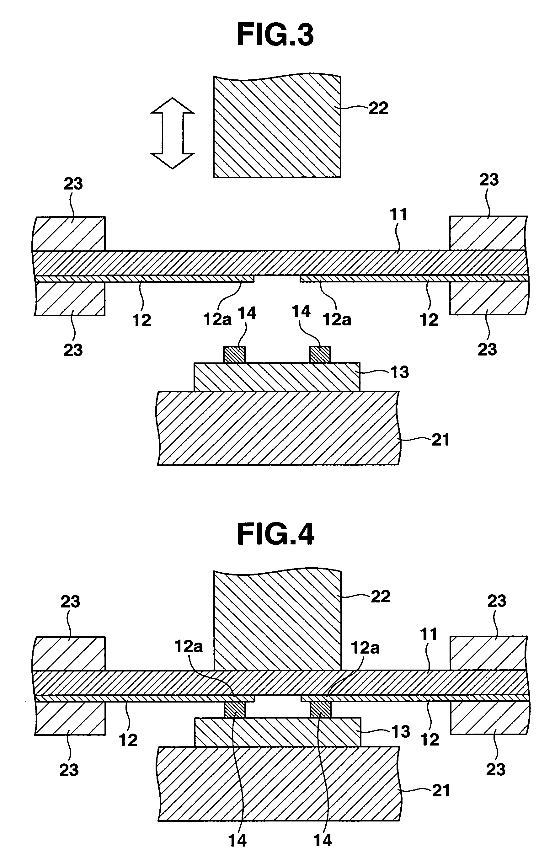
[0212] To manufacture the semiconductor device shown in FIGS. 21 and 22, a bonding apparatus shown in FIGS. 3 and 4 is prepared. In this bonding apparatus, a bonding tool 22 movable in the vertical direction is arranged above a stage 21 having a built-in heater (not shown). A semiconductor chip 13 is placed on the stage 21 with bump electrodes 14 being directed upward. A clamp 23 clamps a wiring board 10 at the periphery of the region where the semiconductor chip 13 is to be mounted. An insulating surface protective film (not shown) of a polyimide resin or epoxy resin is forme...
third embodiment
[0222] The third embodiment of the present invention will be described.
[0223] First, a method of manufacturing a wiring board according to this embodiment will be described with reference to FIGS. 34 to 42.
[0224] As shown in FIG. 34, an Ni film 1 having a thickness of 50 to 125 μm is prepared as a supporting member.
[0225] As shown in FIG. 35, a photosensitive resin layer 2 based on a resin such as a polyimide is formed on the surface of the Ni film 1. The thickness of the photosensitive resin layer 2 is one to three times of the wiring pattern width, and more specifically, about 5 to 30 μm. To form the photosensitive resin layer 2, a known method such as roll coating, spin coating, or casting can be used. After the photosensitive resin is applied, pre-bake is executed in an inert atmosphere at a temperature of about 80° C. to 120° C. to solidify the photosensitive resin and form a film.
[0226] As shown in FIG. 36, a predetermined glass mask 3 appropriate for the purpose is prepar...
PUM
 Abstract
Description
Claims
Application Information
 - R&D
- Intellectual Property
- Life Sciences
- Materials
- Tech Scout
- Unparalleled Data Quality
- Higher Quality Content
- 60% Fewer Hallucinations
Browse by: Latest US Patents, China's latest patents, Technical Efficacy Thesaurus, Application Domain, Technology Topic, Popular Technical Reports.
© 2025 PatSnap. All rights reserved.Legal|Privacy policy|Modern Slavery Act Transparency Statement|Sitemap|About US| Contact US: help@patsnap.com


