Method for forming a trench in a layer or a layer stack on a semiconductor wafer

Inactive Publication Date: 2005-05-19
POLARIS INNOVATIONS
View PDF7 Cites 16 Cited by
  • Summary
  • Abstract
  • Description
  • Claims
  • Application Information

AI Technical Summary

Benefits of technology

[0010] In one aspect, the present invention provides a method to fabricate insulated or semi-insulated trenches with a high degree of uniformity with regard to trench widths formed. The cost investment is lowered in comparison with the prior art. Also, the minimum trench widths that can be achieved are reduced further. The availability of equipment, for example for memory fabrication, is improved by the use of conventional projection apparatuses.
[0019] Preferably using a positive resist, a resist ridge, i.e., a line, is formed in the photosensitive resist. The resist ridge serves as a mask with respect to dopant particles that are subsequently to be implanted. This makes use of the effect whereby the material of the underlying layer, in a part shaded by the resist ridge, can be etched selectively with respect to the implanted part. The consequently patterned underlying layer is itself in turn used as a hard mask layer. The hard mask layer is used as a mask with respect to the underlying layer or layer stack that is actually to be patterned. Consequently, from the resist ridge that has been formed as a line in the photosensitive resist, in a type of tone reversal, it is possible to form an opening in the hard mask layer and subsequently a trench with high dimensional accuracy and uniformity in the case of small structure dimensions in the layer or a layer stack.
[0022] In accordance with a particularly advantageous refinement of the aspect of tone reversal, the resist ridge formed photolithographically is exposed to an oxygen plasma prior to the implantation in a so-called O2 flash, so that its width can be reduced in a controlled manner depending on the duration and the intensity of the plasma process. The combination of tone reversal with such a shrink process of resist ridges makes it possible to form trenches having widths down to 50-60 nm.
[0026] The invention in accordance with the aspect of tone reversal proves to be able to be realized particularly cost-effectively. No deposition and thus no formation of spacers are necessary. It is possible to make relaxed requirements of the selection of the projection apparatuses, and the tone reversal is implemented particularly dimensionally accurately on account of the generally small extent of lateral scattering of dopant particles during the implantation step. The resists that are currently used are formed with resist thicknesses, for example starting from 100 nm, which enable a sufficient absorption of the dopant particles in the implantation step. Consequently, there is no need to make any additional requirements of the resist for carrying out the implantation.

Problems solved by technology

Forming lines or gaps with extremely small structure widths represents one of the major challenges in the fabrication of integrated circuits.
This is caused by fundamental optical effects, which adversely affect the result to a lesser extent precisely in the case of insulated or semi-insulated lines.
However, the requisite outlay is very high, in particular the costs of such projection apparatuses also playing an important part.
Moreover, the process window that can also be achieved with these apparatuses is very small on account of the property of the trenches that the latter are present in insulated or semi-insulated fashion, and this may give rise to bridges in the resist and / or poor contrast in the image produced in the resist.
Therefore, a lithography with projection apparatuses having the 157 nm or 193 nm wavelength does not constitute a suitable solution approach.
However, such techniques are not yet entirely mature at the present time, with the result that intolerable CD variations (CD: critical dimension) may occur precisely in the limit range of extremely minimal structure widths.
However, it is not the exposed regions around the line, but rather the unexposed regions of the line itself, which are stripped out in the subsequent development process.
The advantage that occurs due to the reduction of the fundamental optical effects mentioned above is cancelled, however, by the disadvantage of the unfavorable resolution properties that are inherent to all known and commercially available negative resists.
In the case of this solution approach, too, the costs are very high because it is necessary to introduce an additional deposition and etching process in the fabrication sequence.
Consequently, tolerances that are usually prescribed can often no longer be complied with.
Moreover, the additional deposition and etching processes lead to contamination problems.

Method used


Image

  • Method for forming a trench in a layer or a layer stack on a semiconductor wafer
  • Method for forming a trench in a layer or a layer stack on a semiconductor wafer
  • Method for forming a trench in a layer or a layer stack on a semiconductor wafer

Examples


Embodiment Construction

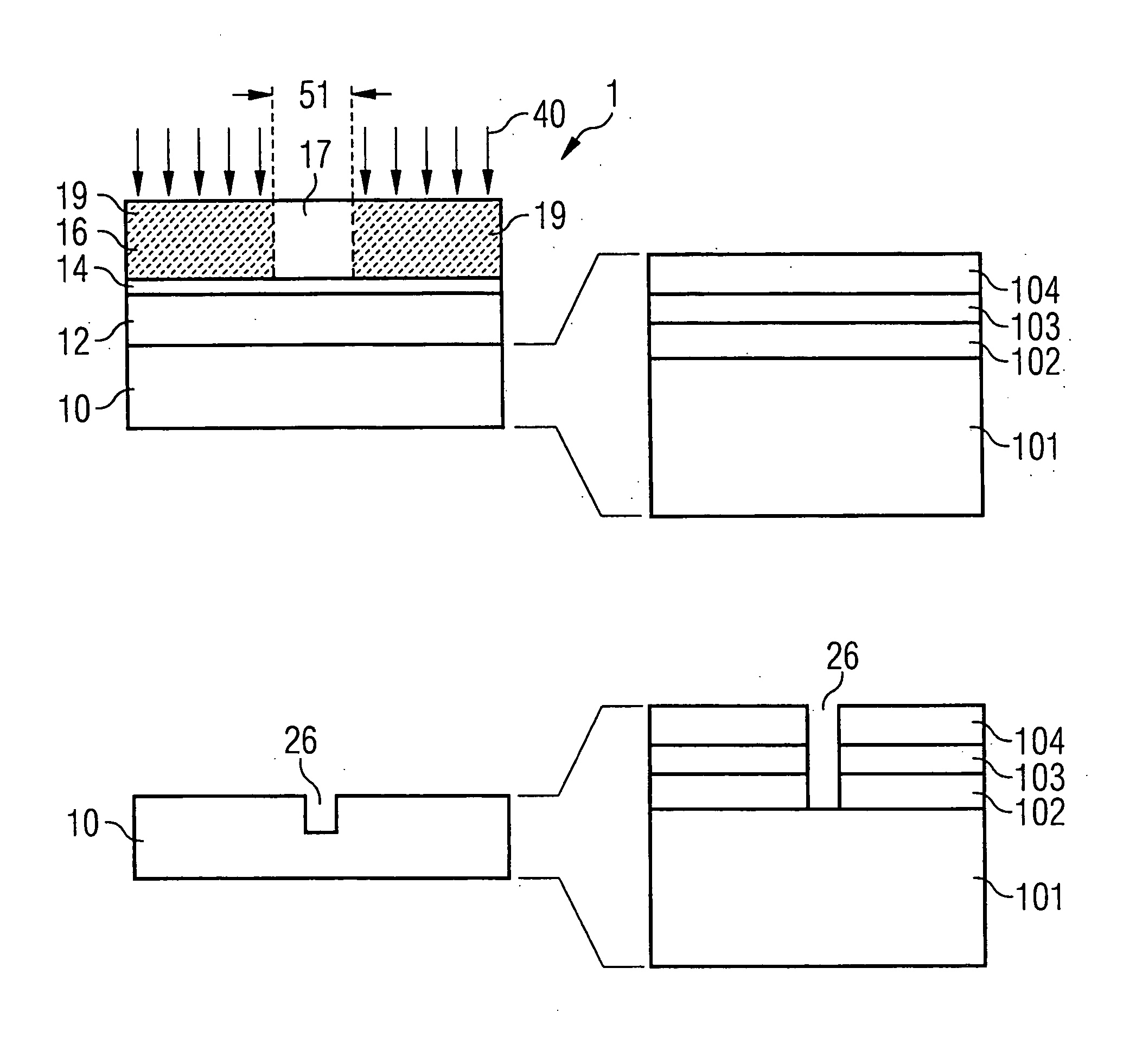
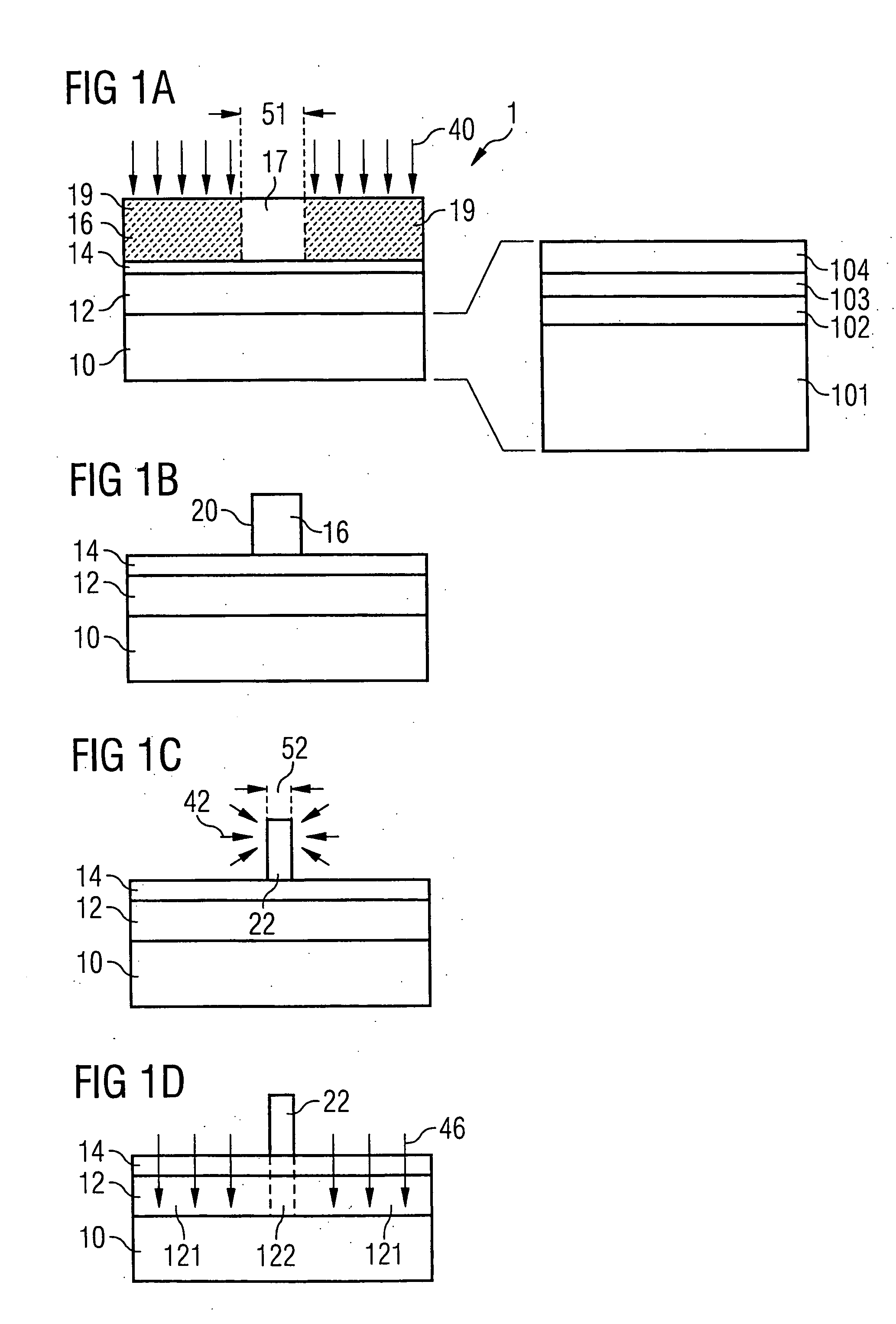
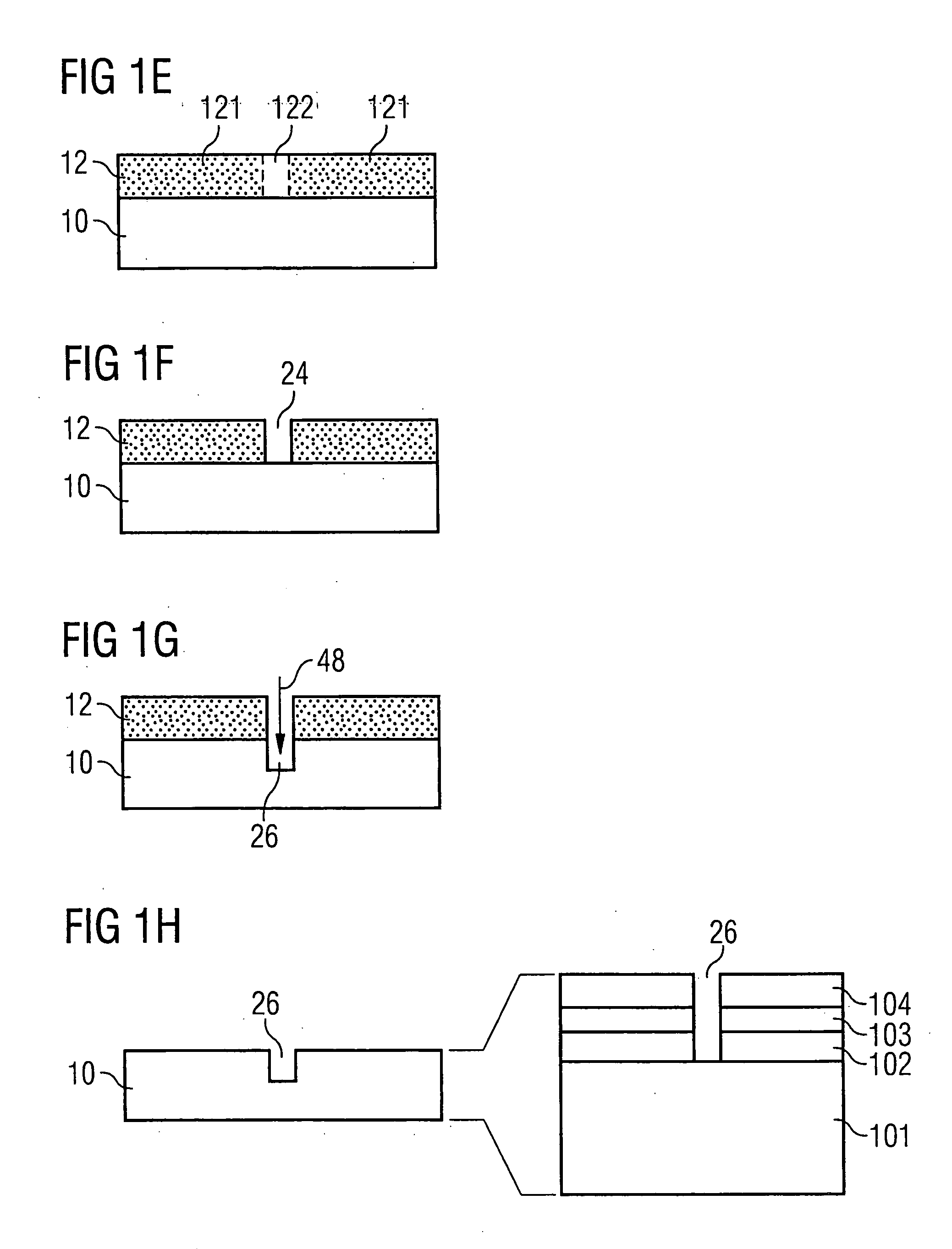
[0032]FIG. 1 shows a first exemplary embodiment of the method according to the invention in a sequence of process steps. FIG. 1a illustrates the state after the provision of a semiconductor wafer 1 when carrying out an exposure step 40. The semiconductor wafer 1 comprises a coated substrate 10, a hard mask layer 12, an antireflection layer 14 (ARC, antireflection coating) and also a photosensitive resist 16, which is a positive resist. In the case of a positive resist, exposed resist portions are stripped out in a developer step.

[0033] The enlargement on the right-hand side of FIG. 1a diagrammatically shows the construction of the coated substrate 10. Situated on the silicon substrate 101 is a layer stack, comprising a first oxide layer 102, a nitride layer 103 and a second oxide layer 104. The layers 102-104 form a layer stack, a so-called ONO layer. Such a layer stack may be used for example for the nonvolatile storage of electrical charges in NROM memories.

[0034] The hard mask ...


PUM


Abstract

Preferably using a positive resist, a resist ridge (20) is formed in a photosensitive resist (16) applied on a semiconductor wafer (1) above a hard mask layer (12). The resist ridge (20) serves as a mask for a subsequent implantation step (46). This makes use of an effect whereby the material of the hard mask layer (12), in a part (122) shaded by the resist ridge (20), can be etched out selectively with respect to the implanted part (121). The consequently patterned hard mask layer is used as an etching mask with respect to an underlying layer or layer stack (102-104) that is actually to be patterned. From the resist ridge (10) that has been formed as a line in the photosensitive resist (16), in a type of tone reversal, an opening (24) has been formed in the hard mask layer and a trench (26) has been formed in the layer / layer stack (102-104). According to the invention, the width (51, 52) of the resist ridge (20) is reduced by exposing the resist ridge (20) to an oxygen plasma (42). As a result, it is possible to form a trench (26) in the hard mask layer (12) and in the layer / layer stack (102-104) the width (52) of which trench is smaller than the lithographic resolution limit during the lithographic patterning of the resist (16).

Description

[0001] This application claims priority to German Patent Application 103 41 321.9, which was filed Sep. 8, 2003 and is incorporated herein by reference. TECHNICAL FIELD [0002] The invention relates to a method for forming a trench in a layer or a layer stack on a semiconductor wafer. The invention relates in particular to the patterning of insulated trenches or gaps in a photosensitive resist arranged on the wafer, and to the transfer thereof into an underlying layer or layer stack with the aid of an etching process. BACKGROUND [0003] Forming lines or gaps with extremely small structure widths represents one of the major challenges in the fabrication of integrated circuits. This applies in particular to the fabrication of memory cell arrays with volatile or non-volatile memory concepts. If the minimum structure widths of insulated or semi-insulated line structures that can be achieved in the course of processing are compared with those of insulated or semi-insulated trench structure...

Claims


Application Information

Patent Timeline
IPC IPC(8): H01L21/027H01L21/033H01L21/302H01L21/308H01L21/461H01L21/8236H01L21/8246H01L21/8247
CPCH01L21/0274H01L21/0337Y10S438/924H01L27/11568H01L21/3086H10B43/30
Inventor SCHROEDER, UWE PAULGOLDBACH, MATTHIASMONO, TOBIAS
Owner POLARIS INNOVATIONS
Why Eureka
Try Eureka