Method of defining forbidden pitches for a lithography exposure tool

a lithography exposure and tool technology, applied in the field of semiconductor device fabrication, can solve the problems of inability to print main features, undesirable variation of feature cds,

Inactive Publication Date: 2005-04-21
TAIWAN SEMICON MFG CO LTD
View PDF7 Cites 8 Cited by
  • Summary
  • Abstract
  • Description
  • Claims
  • Application Information

AI Technical Summary

Benefits of technology

[0009] In accordance with yet another aspect of the present invention, a method of constraining a design rule relating to fabrication of semiconductor devices is provided. This method includes the following steps, the order of which may vary. A set of exposure conditions is selected. A simulation of an actual lithographic exposure process is performed using a computer model. The performing of the simulation includes: selecting a set of pattern pitches for a certain target critical dimension, and running the computer model that simulates an exposure tool using the selected set of exposure conditions for at least some of the pattern pitches from the set of pattern pitches to obtain a corresponding set of depth-of-focus (DOF) values for each pitch ran. It is determined whether the DOF values are greater than a focus budget of the exposure tool for a set of frequently used pitches. If the DOF values are not greater than the focus budget of the exposure tool for the set of frequently used pitches, a new set of exposure conditions is selected and the simulation is re-performed using the new set of exposure conditions. If the DOF values are greater than the focus budget of the exposure tool for the set of frequently used pitches, a verification test is performed. The verification test includes: providing a test mask having formed therein at least one of the pattern pitches used in a last performed simulation; exposing a wafer through the test mask using the exposure tool and using the set of exposure conditions of the last performed simulation; and determining an actual DOF value for at least one of the exposed pattern pitches. One or more forbidden pitch ranges is defined based on the actual DOF values from the verification test performed. The defining of each forbidden pitch range includes: for at least some of the exposed pattern pitches, comparing the corresponding actual DOF value with the focus budget of the exposure tool; if the actual DOF value is not greater than the focus budget of the exposure tool, designating that actual DOF value's corresponding pattern pitch as a forbidden pitch; identifying groups of adjacent forbidden pitches, if any; and forming the forbidden pitch range based on the identified groups of adjacent forbidden pitches. The information regarding the defined forbidden pitch range(s) is integrated into the design rule such that the defined forbidden pitch range(s) may be restricted from use.

Problems solved by technology

The OPE becomes intolerable or unacceptable in some cases for leading edge sub-exposure-wavelength production processes.
One of the primary problems caused by such OPEs is an undesirable variation in feature CDs.
This observation indicates that the existence of the neighboring feature is not always beneficial for main feature printing.
Thus, the forbidden pitch phenomenon has become a limiting factor in advanced photolithography.

Method used


Image

  • Method of defining forbidden pitches for a lithography exposure tool
  • Method of defining forbidden pitches for a lithography exposure tool
  • Method of defining forbidden pitches for a lithography exposure tool

Examples


Embodiment Construction

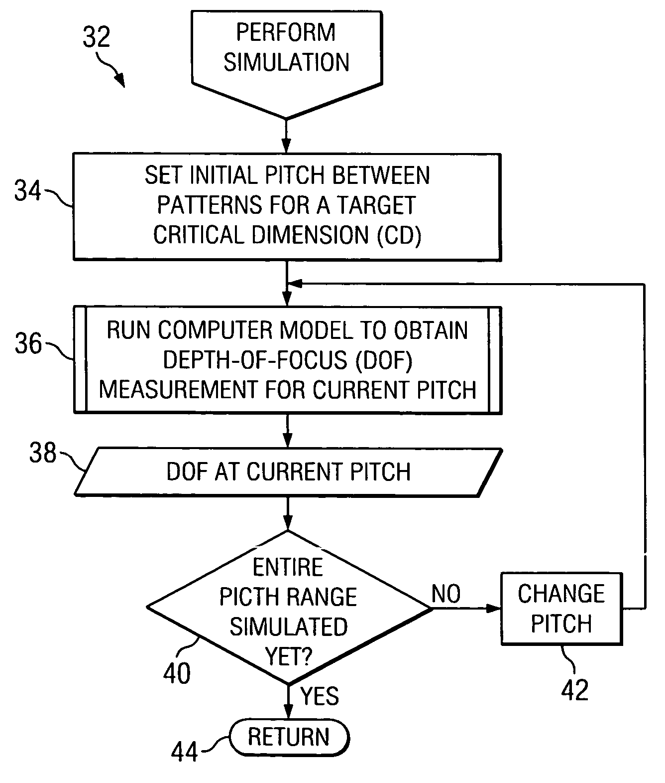
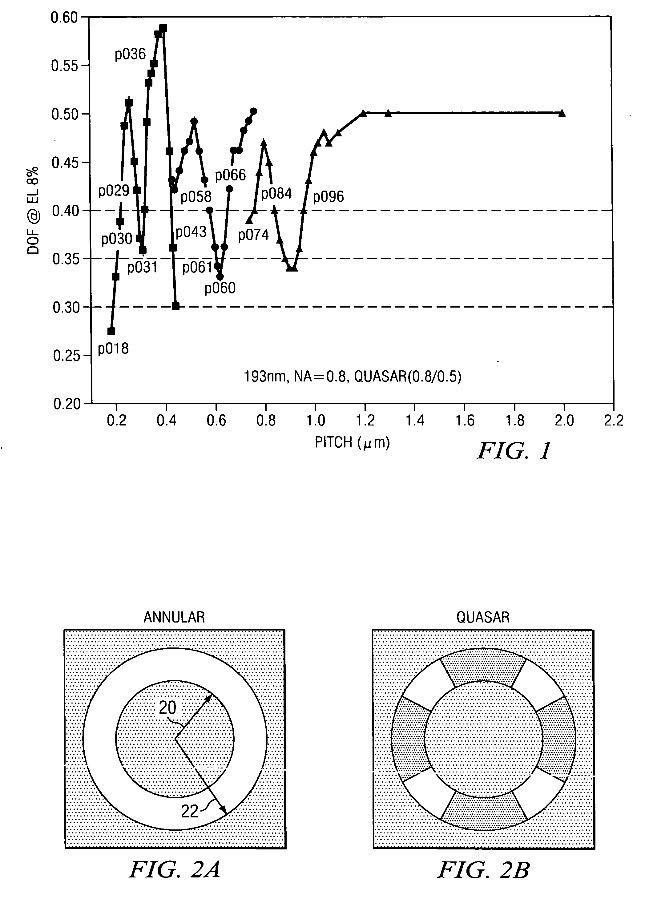
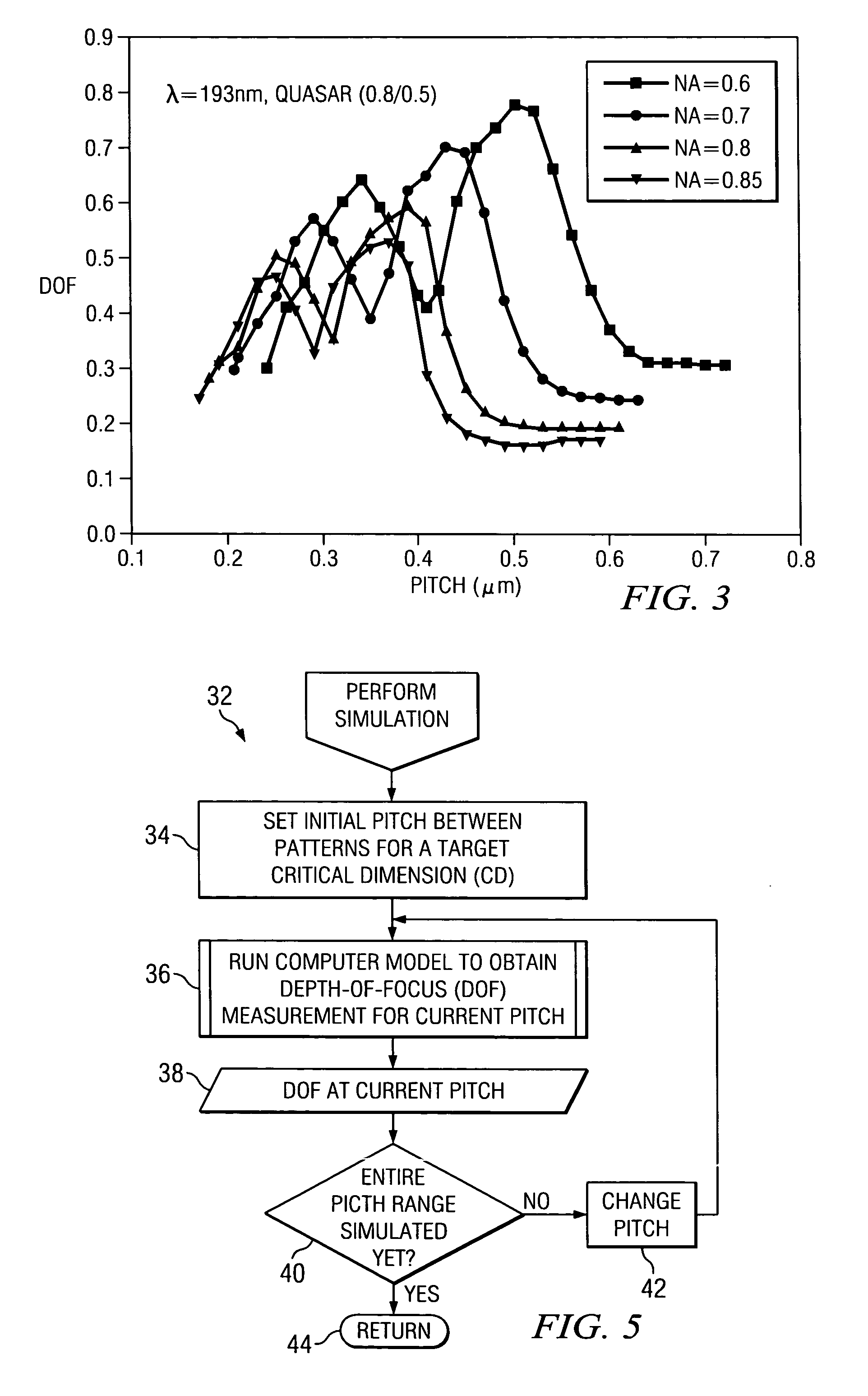
[0015] Referring now to the drawings, wherein like reference numbers are used herein to designate like elements throughout the various views, an illustrative embodiment of the present invention is shown and described. The figures are not necessarily drawn to scale, and in some instances the drawings have been exaggerated and / or simplified in places for illustrative purposes only. One of ordinary skill in the art will appreciate the many possible applications and variations of the present invention based on the following illustrative embodiment of the present invention.

[0016] A semiconductor device foundry often manufactures many different types and generations of devices. Hence, it is desirable that the process windows for lithography processes using existing exposure tools be large enough to cover many kinds of layout patterns while following the design rules for each technology generation. However, the lithography process window of current or prior technology generations may not ...


PUM

PropertyMeasurementUnit
wavelengthaaaaaaaaaa

Abstract

A method of identifying and defining forbidden pitches or forbidden pitch ranges for a lithographic exposure tool under a given set of exposure conditions is provided. In the method, a computer simulation is performed, and its results are compared to frequently used pitches to see if such frequently used pitches may yield depth-of-focus (DOF) values greater than the focus budget for the exposure tool. If so, a verification test is performed by using a test mask and actually exposing a surface with the same pattern pitches simulated. From this, actual DOF values are obtained and compared to the focus budget of the exposure tool. Any pitches having a DOF value greater than the focus budget are designated as forbidden pitches. This forbidden pitch information may be integrated into a design rule to restrict the use of such forbidden pitches under the given exposure conditions where they are likely to arise.

Description

TECHNICAL FIELD [0001] The present invention generally relates to the fabrication of semiconductor devices. In one aspect it relates more particularly to a method of constraining chip design rules from the use of identified / defined forbidden pitches and / or forbidden pitch ranges. BACKGROUND [0002] Lithographic processes are often used in the manufacture of integrated circuits (ICs) for semiconductor devices. In such processes, a mask having a circuit pattern corresponding to an individual layer of an IC is typically used. In such case, a projection beam of radiation may be used to image this mask pattern onto various target portions on a wafer (e.g., silicon wafer, silicon-on-insulator wafer) that has been coated with a layer of radiation-sensitive material (e.g., photoresist material). Such techniques are widely known in the art of semiconductor manufacturing. [0003] Lithographic apparatus may employ various types of projection radiation, such as (but not necessarily limited to): u...

Claims


Application Information

Patent Timeline
Patent Type & Authority Applications(United States)
IPC IPC(8): G03F1/14G03F7/20G06F17/50
CPCG03F1/14G03F7/70425G03F7/70641G03F7/705G03F7/70433G03F1/44
Inventor SHIN, JAW-JUNGCHEN, CHUN-KUANGGAU, TSAI-SHENGLIN, BURN-JENGTIEN, LI-CHUNCHANG, MI-CHANGCHOU, YU-JUNYOU, JAN-WENSHU, KING-CHANGCHEN, LI-JUI
Owner TAIWAN SEMICON MFG CO LTD
Why Eureka
Try Eureka