
Dielectric materials and methods for integrated circuit applications

a technology of integrated circuits and materials, applied in the direction of material analysis, instruments, and semiconductor/solid-state device details, can solve the problems of reliability failure, increased softness, and increased softness, and achieve the effect of reducing the number of processing steps, reducing the sensitivity of fhosm, and reducing costs

Inactive Publication Date: 2005-02-10
SILECS OY
View PDF7 Cites 28 Cited by
  • Summary
  • Abstract
  • Description
  • Claims
  • Application Information

AI Technical Summary

Benefits of technology

In a still further embodiment of the invention, an integrated circuit device is provided having a substrate and areas of electrically insulating and electrically conductive material, wherein the electrically insulating material is a hybrid organic-inorganic material that has a coefficient of thermal expansion in the range of 12-22 ppm and a modulus of 4.0 GPa or more.
In yet another embodiment of the invention, an integrated circuit device is provided comprising a substrate and areas of electrically insulating and electrically conductive material, wherein the electrically insulating material is a hybrid organic-inorganic material that has a coefficient of thermal expansion of 12 to 22 ppm, a density of 1.2 g / cm3 or more, and a dielectric constant of 3.0 or less.
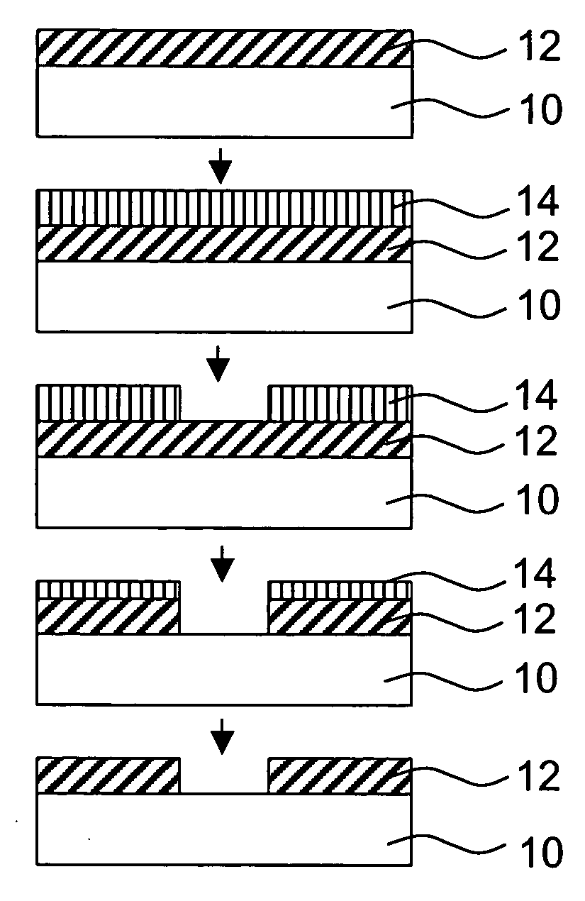
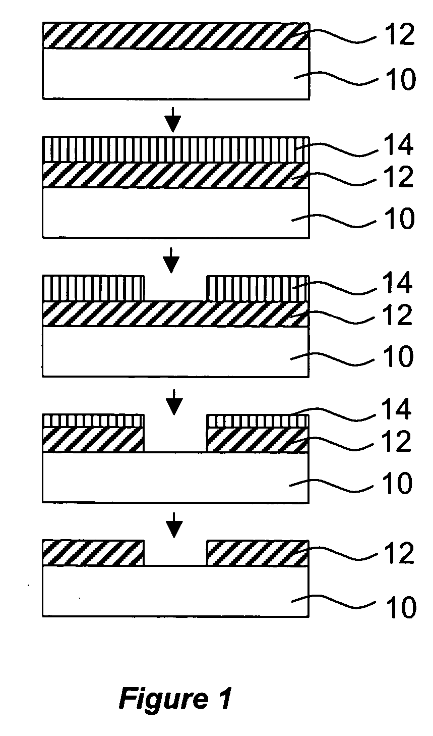
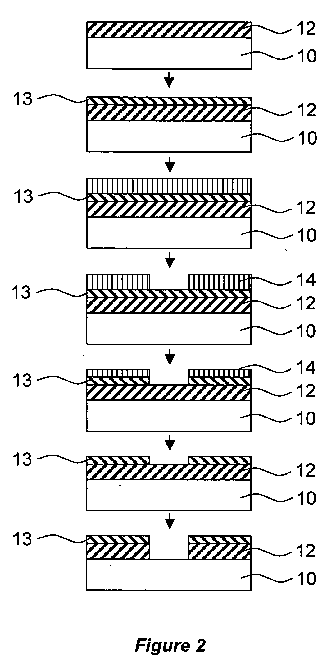
In another embodiment of the present invention, precursors, as described above, are used to make fully, partially and non-fluorinated hybrid organic-inorganic siloxane materials (FHOSM) as an interlevel dielectric and / or hard mask in integrated circuit processes and devices. In one embodiment of the invention, the FHOSM takes the place of the typical interlevel dielectric or hard mask films depicted in FIGS. 1-3. Application of the IC material of the invention is performed with spin-on or other deposition processes. Patterning can be accomplished by masking and etching procedures described previously. Or, the sensitivity of FHOSM can be utilized to reduce the number of processing steps. Instead of patterning the film with photoresist and etch processes, the film dielectric itself is photopatternable like photoresist. Compared to the standard process depicted in FIG. 1, the photopatternable FHOSM process eliminates several processing steps potentially reducing costs and improving yield. Similar to the photopatternable dielectric concept described in the previous embodiment, a photopatternable FHOSM may be used as a hard mask material for etching semiconductor, dielectric, or metal underlayers. The number of processing steps required to fabricate the feature is reduced with respect conventional processing techniques shown in FIG. 1. And, owing to their “negative” behavior under exposure, photopatternable FHOSM can also be applied to reduce the number of processing steps required to build a dielectric “dual damascene” structure. In addition, to pattering FOSHM by photolithography processes defined previously, exposure by particle beams, such as electron beams, is also possible. Also, the present invention covers use of FOSHM in printed circuit board applications, which are similar to those discussed for integrated circuits.

Problems solved by technology

Silicate-based low-k materials can demonstrate exceptional thermal stability and usable modulus but can be plagued by brittleness and cracking.
Organic materials, by contrast, often show improved material toughness, but at the expense of increased softness, lower thermal stability, and higher thermal expansion coefficients.
Porous materials sacrifice mechanical properties and possess a strong tendency of absorbing chemicals used in semiconductor fabrication leading to reliability failures.
Fluorinated materials can induce corrosion of metal interconnects, rendering a chip inoperative.
Generally, the mechanical robustness and thermal conductivity of low-k materials is lower than the corresponding properties of their pure silicon dioxide analogues, making integration into the fabrication flow very challenging.
Further, known materials comprising exclusively inorganic bonds making up the siloxane matrix are brittle and have poor elasticity at high temperatures.
The procedures shown in FIGS. 1-3 are often repeated many times during integrated circuit application, which adds to the cost of the circuit and degrades yield.

Method used


Image

  • Dielectric materials and methods for integrated circuit applications
  • Dielectric materials and methods for integrated circuit applications
  • Dielectric materials and methods for integrated circuit applications

Examples


example vi

COMPOUND EXAMPLE VI

In another compound example, a compound is provided of the general formula: R1R2MXOR3, where R1 is any partially or fully fluorinated organic group (preferably a partially or fully fluorinated aryl, alkenyl, alkynyl or alkyl group) as set forth above with respect to R1, R2 is any partially or fully fluorinated organic group (preferably a partially or fully fluorinated aryl, alkenyl, alkynyl or alkyl group) as set forth above with respect to R1, or any such organic groups nonfluorinated, and where R1 and R2 are the same or different from each other, where M is an element selected from group 14 of the periodic table as mentioned above, where OR3 is an alkoxy group as above, and where X is a halogen. R1 and R2 can be the same or different from each other. Specific examples within this category include:

example vii

COMPOUND EXAMPLE VII

In a further compound example, a compound is provided of the general formula: R1 R2MX2, where R1 is any partially or fully fluorinated organic group (preferably a partially or fully fluorinated aryl, alkenyl, alkynyl or alkyl group) as set forth above with respect to R1, R2 is any partially or fully fluorinated organic group (preferably a partially or fully fluorinated aryl, alkenyl, alkynyl or alkyl group) as set forth above with respect to R1, or any such organic groups nonfluorinated, and where R1 and R2 are the same or different from each other, where M is an element selected from group 14 of the periodic table as mentioned above, and where X is a halogen as above—Except where M is Si, R1 and R2 are perfluorinated phenyl, and X is Cl, which, though not novel per se, is novel when used as part of the methods for making the materials of the invention as will be discussed further below. Specific examples within this category include:

As Compounds V-VII have t...

example 1

Making a Compound I via Method B

CF2═CF—Cl+sec / tert-BuLi→CF2═CF—Li+BuCl

CF2═CF—Li+Si(OEt)4→CF2═CF—Si(OEt)3+EtOLi

200 ml of freshly distilled dry Et2O is added to a 500 ml vessel (under an argon atmosphere). The vessel is cooled down to −80° C. and 15 g (0.129 mol) of CF2═CFCl gas is bubbled to Et2O. 100 ml (0.13 mol) of sec-BuLi is added dropwise during three hours. The temperature of the solution is kept below −60° C. all the time. The solution is stirred for 15 minutes and 29 ml (27.08 g, 0.130 mol) of Si(OEt)4 is added in small portions. The solution is stirred for over night allowing it to warm up to room temperature. Formed red solution is filtered and evaporated to dryness to result crude trifluorovinyltriethoxysilane, CF2═CFSi(OEt)3.


PUM

PropertyMeasurementUnit
densityaaaaaaaaaa
temperatureaaaaaaaaaa
dielectric constantaaaaaaaaaa

Abstract

An integrated circuit device is provided having a substrate and areas of electrically insulating and electrically conductive material, where the electrically insulating material is a hybrid organic-inorganic material that requires no or minimal CMP and which can withstand subsequent processing steps at temperatures of 450° C. or more.

Description

BACKGROUND OF THE INVENTION Built on semiconducting substrates, integrated circuits comprise millions of transistors and other devices, which communicate electrically with one another and with outside packaging materials through multiple levels of vertical and horizontal wiring embedded in a dielectric material. Within the multilayer metallization structure, “vias” make up the vertical wiring, whereas “interconnects” form the horizontal wiring. Fabricating the metallization can involve the successive depositing and patterning of multiple layers of dielectric and metal to achieve electrical connection among transistors and to outside packaging material. The patterning for a given layer is often performed by a multi-step process comprising layer deposition, photoresist spin, photoresist exposure, photoresist develop, layer etch, and photoresist removal on a substrate. Alternatively, the metal may sometimes be patterned by first etching patterns into a layer of a dielectric material, ...

Claims


Application Information

Patent Timeline
Patent Type & Authority Applications(United States)
IPC IPC(8): G01N27/00
CPCH01L21/02126H01L21/02216H01L21/02282H01L21/3122H01L21/76802H01L21/76808H01L2924/12044H01L21/76829H01L21/76835H01L23/5329H01L2221/1031H01L2924/09701H01L21/7681H01L2924/0002H01L2924/00
Inventor RANTALA, JUHA T.HACKER, NIGELREID, JASONMCLAUGHLIN, WILLIAMTORMANEN, TEEMU T.
Owner SILECS OY
Learn More