Electrostatic chuck
- Summary
- Abstract
- Description
- Claims
- Application Information
AI Technical Summary
Benefits of technology
Problems solved by technology
Method used
Image

Examples
example 1
(Example 1)
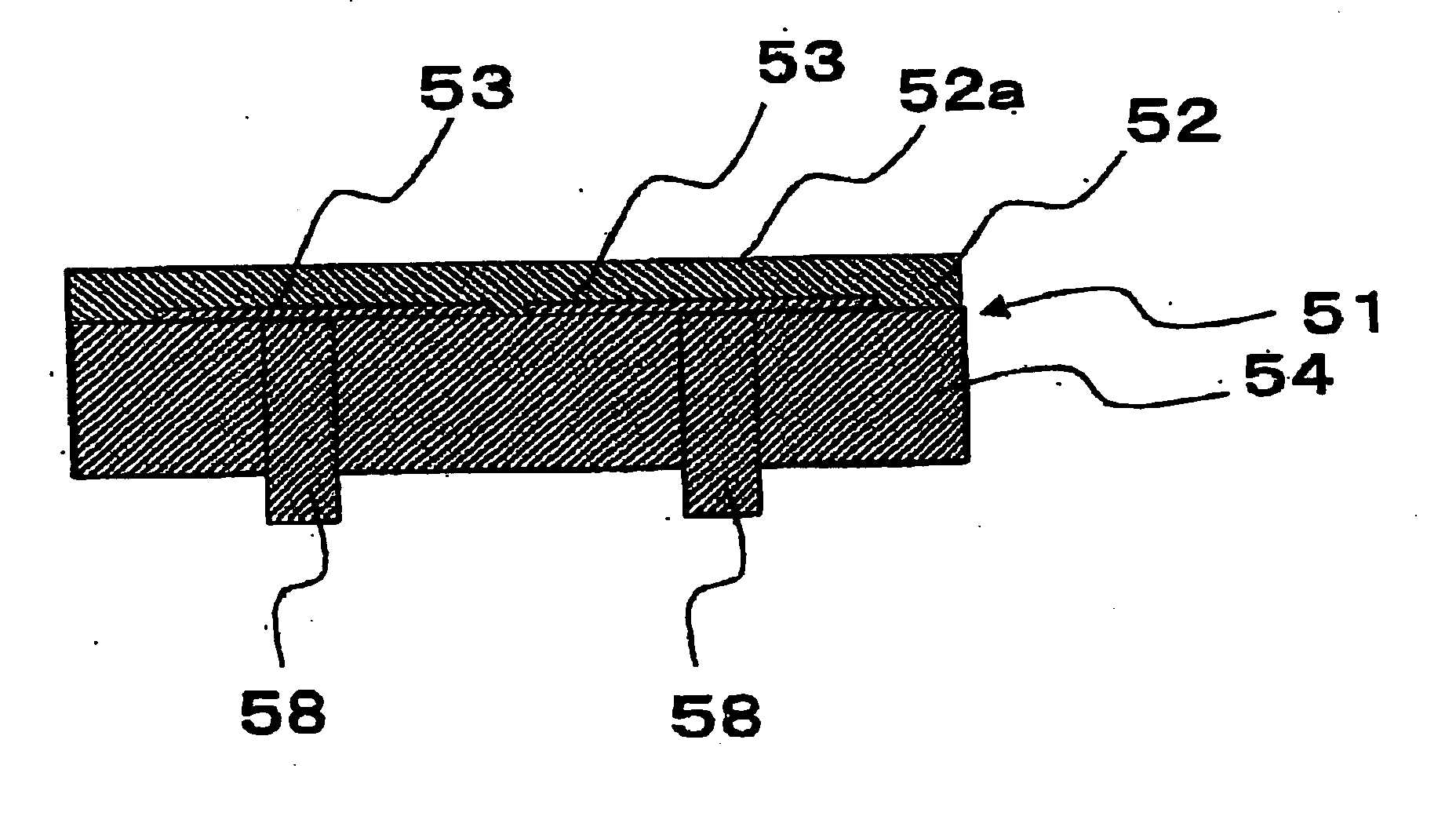
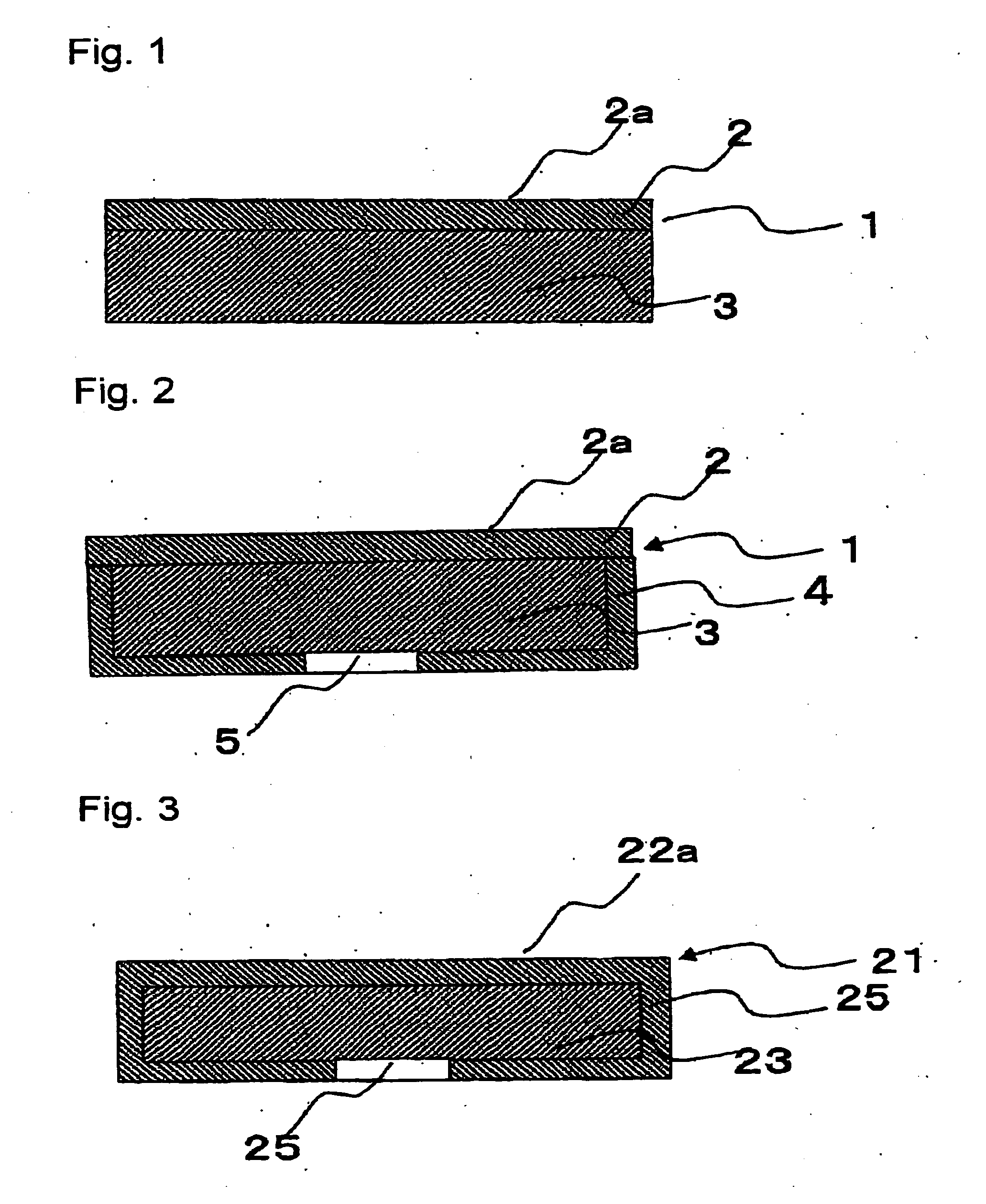
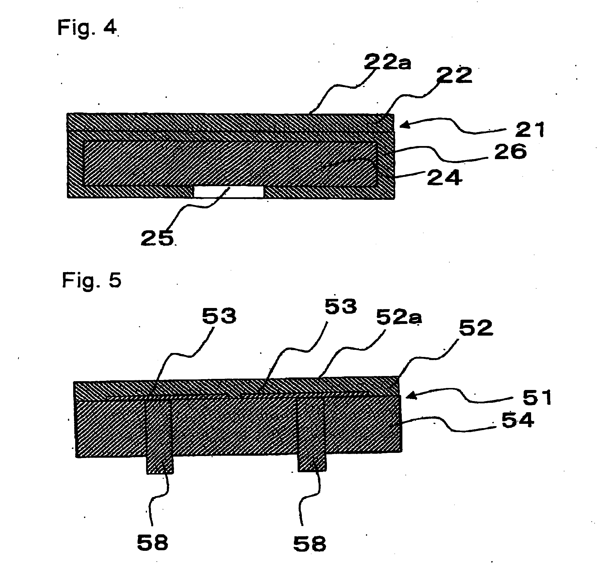
[0086] A porous body of SiC with a diameter of 198 mm and a thickness of 5 mm was impregnated with aluminum alloy to form a layer of aluminum alloy with a thickness of 1 mm on the side face and the top and bottom faces, obtaining the conductive base 3 with a diameter of 200 mm and a thickness of 7 mm, which contained 80 mass % of SiC and 20 mass % of aluminum alloy. Next, an insulating film of a ceramics was formed on the top surface to make samples of No. 1 to 10, which were evaluated on items of insulation breakdown, cracking, flaking, plasma-resistance of the insulating film.
[0087] The insulation breakdown of the insulating film was evaluated in whether the insulation was broken down or not when a voltage of 3 kV was applied between the wafer and the conductive base 3.
[0088] Further, regarding the evaluation on the plasma-resistance of the insulating film, the placing surface was exposed for 100 hours in plasma which was generated between the placing surface and an o...
example 2
[0098] Secondly, using the conductive base 3 with a diameter of 200 mm and a thickness of 7 mm as used in Experiment 1, and an insulating film 2 of amorphous aluminum oxide, various films were deposited while changing the amount of argon contained in the amorphous ceramic insulating film 2 under various deposit conditions. Whether flaking and cracking occurred or not was evaluated.
TABLE 2sampleamount ofcracking,insulation breakdownNo.argon (atom %)flakingof insulating film210.5yes—221nono233nono246nono2510nono
[0099] The sample No. 21, which had the smaller amount of argon of 0.5 atom %, showed cracking occurred in the insulating film.
[0100] However, the samples No. 22 to 25, which had the amount of argon of 1 to 10 atom % according to the present invention, showed no cracking and no insulation breakdown occurred in the insulating film. Therefore, it can be seen that the amount of argon is preferably 1 to 10 atom %.
[0101] Next, using the conductive base 3 with a diameter of 200 m...
example 3
[0106] Samples No. 41 to 44, in which material of the insulating film of amorphous ceramics was aluminum oxide, yttrium oxide, yttrium-aluminum oxide, or cerium oxide, respectively, and a comparative sample No. 45, in which the insulating film was formed of polycrystal alumina, were exposed in plasma, then each etching rate of the insulating film was compared.
[0107] In the evaluation way, in a state that the outer circumferential top face and the side face of the electrostatic chuck were provided with a cover ring to cover areas having no insulating film, the surface of the insulating film was exposed in plasma. Regarding the plasma condition, the insulating film was exposed for 2 hours in plasma which was generated between the placing surface and an opposite electrode, which was located above the placing surface, by supplying a radio frequency power of 2 kW between the opposite electrode and the conductive base with a halogen gas of Cl2 flowing at 60 sccm and a vacuum degree of 4 ...
PUM
 Abstract
Description
Claims
Application Information
 - R&D
- Intellectual Property
- Life Sciences
- Materials
- Tech Scout
- Unparalleled Data Quality
- Higher Quality Content
- 60% Fewer Hallucinations
Browse by: Latest US Patents, China's latest patents, Technical Efficacy Thesaurus, Application Domain, Technology Topic, Popular Technical Reports.
© 2025 PatSnap. All rights reserved.Legal|Privacy policy|Modern Slavery Act Transparency Statement|Sitemap|About US| Contact US: help@patsnap.com