Method of fabrication of a support structure for a semiconductor device
- Summary
- Abstract
- Description
- Claims
- Application Information
AI Technical Summary
Benefits of technology
Problems solved by technology
Method used
Image
Examples
first embodiment
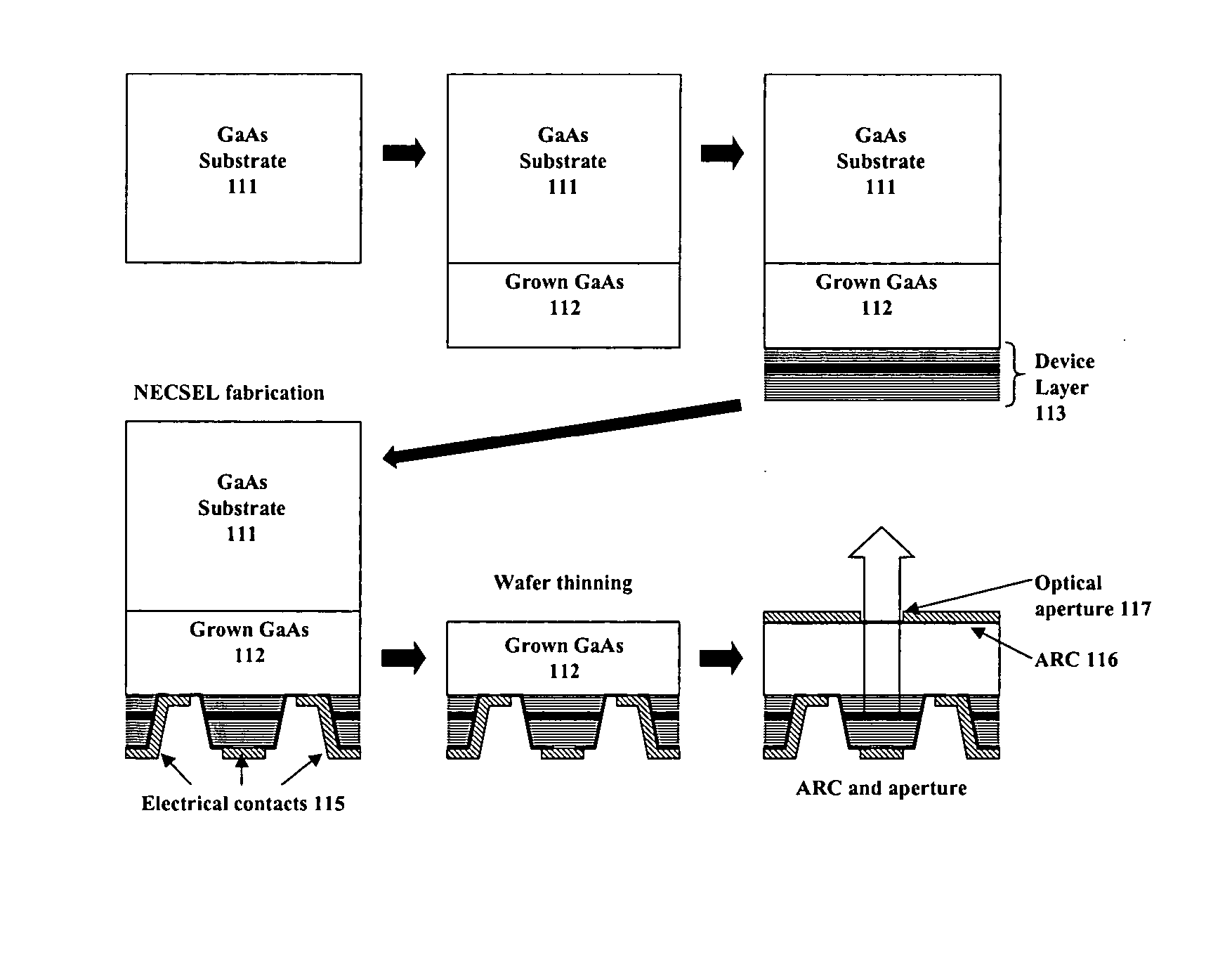
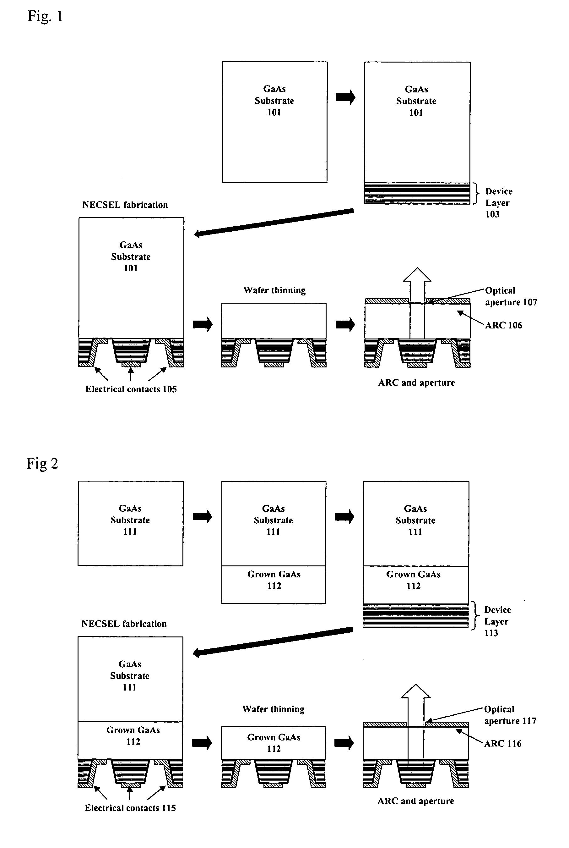
[0019] According to the present invention, the support layer 112 has a uniform doping level of between 5×1016 cm−3 and 5×1017 cm−3 and a thickness of about 100 μm.
second embodiment
[0020] According to the present invention, the support layer 112 is doped very lightly through most of the material (for example, less than 1×1016 cm−3) in order to minimize optical absorption, while a thin (e.g., 2 to 20 μm thick) layer of more heavily doped material (for example, 5×1017 cm−3 and 5×1018 cm−3) is formed immediately adjacent to the device layer to provide electrical conduction. Such a tailored doping profile is readily obtained, for example, by adjusting dopant source flow rates during epitaxial growth by metal organic chemical vapor deposition (MOCVD).
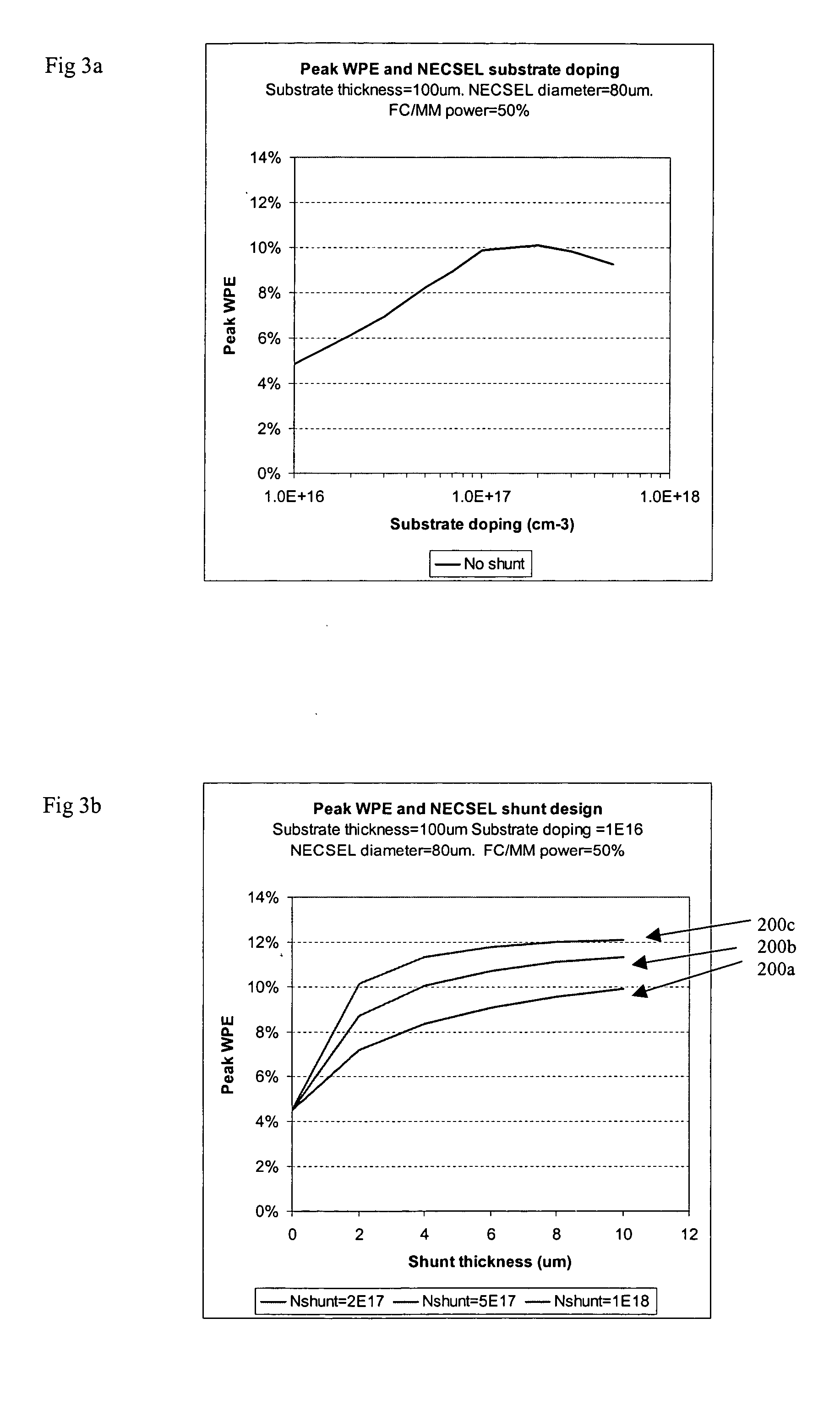
[0021] The effect of tailoring the doping profile in this way can be described in more detail with respect to FIGS. 3a-b. The figures show the modeled wall plug efficiency (WPE) for various NECSEL designs. The wall plug efficiency is the ratio of the optical power emitted by the NECSEL to the input electrical power and is an important performance value for diode lasers. In general, high wall plug efficiency is desired....
PUM
 Abstract
Description
Claims
Application Information
 - R&D
- Intellectual Property
- Life Sciences
- Materials
- Tech Scout
- Unparalleled Data Quality
- Higher Quality Content
- 60% Fewer Hallucinations
Browse by: Latest US Patents, China's latest patents, Technical Efficacy Thesaurus, Application Domain, Technology Topic, Popular Technical Reports.
© 2025 PatSnap. All rights reserved.Legal|Privacy policy|Modern Slavery Act Transparency Statement|Sitemap|About US| Contact US: help@patsnap.com


