Method for manufacturing auxiliary gas-adding polyurethae/polyurethane-urea polishing pad

Inactive Publication Date: 2004-02-05
IV TECH CO LTD
View PDF8 Cites 62 Cited by
  • Summary
  • Abstract
  • Description
  • Claims
  • Application Information

AI Technical Summary

Benefits of technology

[0019] In the manufacture method according to the invention, formulas of polyol resins can be modulated optionally to obtain different hardness, density, elongation and strength for a flexible PU polishing pad with uniform continuous open cells. Besides, with proper mold design and formula modulation of resins containing active hydrogen, single pieces of symmetric foamed PU products can be obtained by the manufacture method according to the invention; such a symmetric foamed PU product is not foamed at surfaces thereof, but formed with continuous symmetric pores gradually away from the surfaces. Each single piece of the symmetric foamed PU product can be cut symmetrically in the middle to form two pieces of dual-layer PU structure, including a relatively more rigid surface layer and a relatively softer buffer layer beneath the surface layer. The rigid surface layer provides the PU polishing pad with better planarity for polishing wafers, and the soft buffer layer provides the PU polishing pad with better uniformity during polishing in facility with foaming agents and auxiliary gases.
[0020] The single-piece auxiliary gas-adding PU polishing pad, fabricated by high-pressure reaction injection molding according to the invention, can be subjected to fine surface treatment to obtain single-layer combined structure of a foamed PU product and a pressure-sensitive tape. This type of polishing pad has appropriate surface hardness to maintain preferable planarity and quality, and surfaces of the polishing pad can properly deform along with chip curvature, so as to achieve better polishing uniformity.

Problems solved by technology

However, for such a multi-layer conductive circuit structure, with increase in number of the conductive circuit layers, corrugation and unevenness of wafer surfaces would become more substantial.
When the polishing pad moves and presses on wafer surfaces, abrasive particles of the slurry in frictional contact with the wafer surfaces lead to the wafers having abrasive loss.
However, too large pores make the polishing pad hardly achieve constant polishing pressure, resulting in low planarity of polished surfaces.
When the polishing pad starts to be "glazing" and is hardly restored with its polishing function by the conditioning process, the polishing pad cannot be used any longer.
However, such polishing pads are fabricated by complex and labor-consuming processes, such as formation of PU foam polymer, surface removal / singulation and attachment to substrates.
And, the processes of surface removal / singulation are not easily controlled, thereby possibly leading to problems of poor uniformity of pores, small surface openings of the pores (i.e. pore bottom larger in diameter than surface opening), increased proportion of pore walls in working surfaces for the polishing pads.
This would be detrimental to polishing stability of the polishing pads, such as unpredictable lifetime, uneven contact between slurry particles and surfaces to be polished, and the like.
Such a fabrication method is not only time-consuming but also hard to retain stable operation conditions, and thus not well applied to the industry.
This patent effectively improves the macro-defects at the polishing surface due to cutting and polishing performance, but the disadvantages such as time-consuming for production and the like still exist in this patent.
Even though this patent can improve flatness of a polished article that can not be obtained by the prior art in which only one type of the microballoons is used, it also retains the problems, such as requirements for heating temperature higher than normal temperature and prolonged curing time, which are detrimental to industrial application.

Method used


Image

  • Method for manufacturing auxiliary gas-adding polyurethae/polyurethane-urea polishing pad
  • Method for manufacturing auxiliary gas-adding polyurethae/polyurethane-urea polishing pad

Examples


example 2

[0029]

3 Formula wt. % Polyester polyol (Mw = 1000) 84 Ethylene glycol 16 Organic amine catalyst 1.0 Water 0.2 Siloxane foam stabilizer 1.0 MDI isocyanate prepolymer (NCO = 29.5%) 100

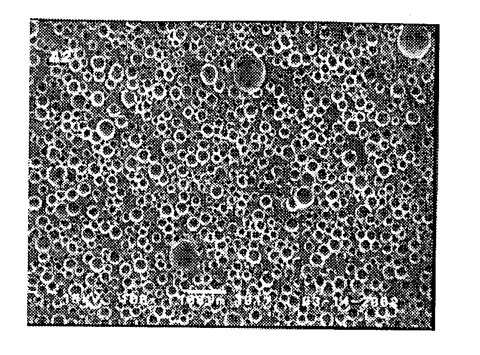
[0030] In Example 2, raw materials are used at 55.degree. C., and incorporated with air of 12 vol. %. Mold temperature is 60.degree. C., and operation pressure of a reaction injection-molding machine is 15 MPa. Bubble continuity and uniformity can be well observed through the use of a scanning electronic microscope (SEM), as shown in FIG. 1. By the above formula and conditions, physical properties of fabricated products are measured as follows.

4 Tensile strength (MPa) 19 Elongation (%) 180 Hardness (shore-D) 60 Density (g / cm.sup.3) 0.7 Compressibility (%) 0.98

example 3

[0031]

5 Formula wt % Polycaprolactone polyester (Mw = 1000) 84 Ethylene glycol 16 Organic amine catalyst 0.45 Pentane 6 Siloxane foam stabilizer 1.0 MDI isocyanate prepolymer (NCO = 28%) 100

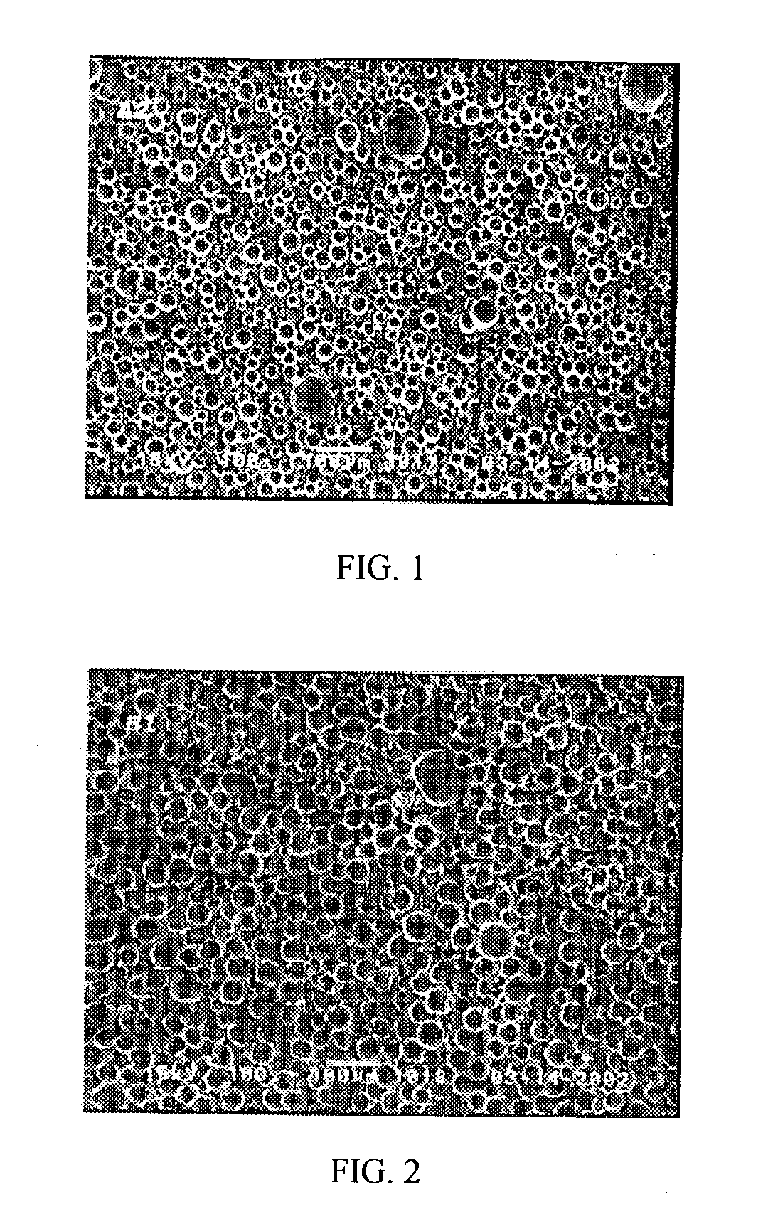
[0032] In Example 3, raw materials are used at 50.degree. C., and incorporated with air of 15 vol. %. Mold temperature is 60.degree. C., and operation pressure of a reaction injection-molding machine is 15 MPa. Bubble continuity and uniformity can be well observed, as shown in FIG. 2. By the above formula and conditions, physical properties of fabricated products are measured as follows.

6 Tensile strength (MPa) 17.8 Elongation (%) 156 Hardness (shore-D) 58 Density (g / cm.sup.3) 0.7 Compressibility (%) 1.01

[0033] In the above examples, by using various chain extender, amount of foaming agent and injected amount into a metallic mold, different density and hardness can be obtained as well as physical properties and parameters can be further modulated for the fabricated PU polishing pad.


PUM

PropertyMeasurementUnit
Linear densityaaaaaaaaaa
Pressureaaaaaaaaaa
Pressureaaaaaaaaaa

Abstract

A method for manufacturing a PU (polyurethane) polishing pad is provided. Resins containing active hydrogen functional groups such as polyol resins, polyamine resins, and polythiol resins, and polyisocyanate resins containing -NCO functional groups are mixed to form a foamed PU polishing pad with excellent polishing properties by reaction injection-molding under high pressure, low temperature and auxiliary gas-adding. The PU polishing pad in accompany with an abrasive slurry can be widely used to polish high-level products such as wafers and optical glass.

Description

[0001] This application claims the priority benefit of Taiwan application serial no. 91117406, fixed Aug. 02, 2002.BACKGROUND OF INVENTION[0002] 1. Field of the Invention[0003] The present invention relates to methods for manufacturing polyurethanes (PUs) and polyurethane-ureas (PURs) polishing pads, and more particularly, to a method for fabricating a multi-functional microcellular PUs and PURs polishing pad for use to polish wafers and optical lenses.[0004] 2. Background of the Invention[0005] To fabricate semiconductor devices such as memory wafer or logic wafer, it is intended to increase aspect ratios and conductive circuit layers for achieving high density of electronic components and reduction in fabrication costs. However, for such a multi-layer conductive circuit structure, with increase in number of the conductive circuit layers, corrugation and unevenness of wafer surfaces would become more substantial. In order to form more conductive circuit layers and to assure product...

Claims


Application Information

Patent Timeline
IPC IPC(8): B24B37/24B24D3/32B24D13/14C08G18/10
CPCB24B37/24B24D3/32C08G18/10C08G18/6564C08G18/664
Inventor SHIH, WEN-CHANGCHANG, YUNG-CHUNGCHU, MIN-KUEIWEI, LUNG-CHENCHEN, WEN-PIN
Owner IV TECH CO LTD
Why Eureka
Try Eureka