
Quartz member for semiconductor manufacturing equipment and method for metal analysis in quartz member

a technology of quartz glass furnace tube and quartz glass, which is applied in the direction of manufacturing tools, instruments, and mechanical means, etc., can solve the problems of extremely coarse detection lower limit, poor quality products, and impartially judging the quality of quartz glass furnace tubes

Inactive Publication Date: 2003-01-02
TOKYO ELECTRON LTD
View PDF3 Cites 35 Cited by
  • Summary
  • Abstract
  • Description
  • Claims
  • Application Information

AI Technical Summary

Benefits of technology

[0016] In the present invention, a surface of the quartz specimen is divided into thin layers to be analyzed, followed by chemically analyzing the respective layers. Accordingly, analysis results of high accuracy can be obtained and the diffusion coefficients of high reliability can result. Thereby, with the material of small diffusion coefficient, a quartz member can be manufactured for semiconductor manufacturing equipment. Accordingly, the quartz member used for semiconductor manufacturing equipment capable of heat treating the semiconductor wafers without contaminating can be obtained.

Problems solved by technology

Therefrom, the metal atoms intrude into a space inside of the quartz glass furnace tube 124 and deposit on the semiconductor wafers 129 being heat treated to cause so-called contamination, thereby resulting in an occurrence of poor quality products.
Accordingly, there is a problem in impartially judging quality of the quartz glass furnace tube that is a product in terms of the data of the diffusion coefficients supplied from the manufacturers.
However, in the SIMS method, a detection lower limit is extremely coarse as 4.8 .mu.g / g, an analysis area (depth) being small as approximately 200 .mu.m.
Accordingly, there are problems that measurement capacity is poor, measurement accuracy being low, investment being large, cost for one measurement being high.
On the other hand, in the optical method, a depth resolution is too thick as 500 .mu.m, the detection lower limit being approximately 10 ng / g.
As a result, both the measurement capacity and measurement accuracy can not be sufficiently satisfied.

Method used


Image

  • Quartz member for semiconductor manufacturing equipment and method for metal analysis in quartz member
  • Quartz member for semiconductor manufacturing equipment and method for metal analysis in quartz member
  • Quartz member for semiconductor manufacturing equipment and method for metal analysis in quartz member

Examples


first embodiment

[0060] (First Embodiment)

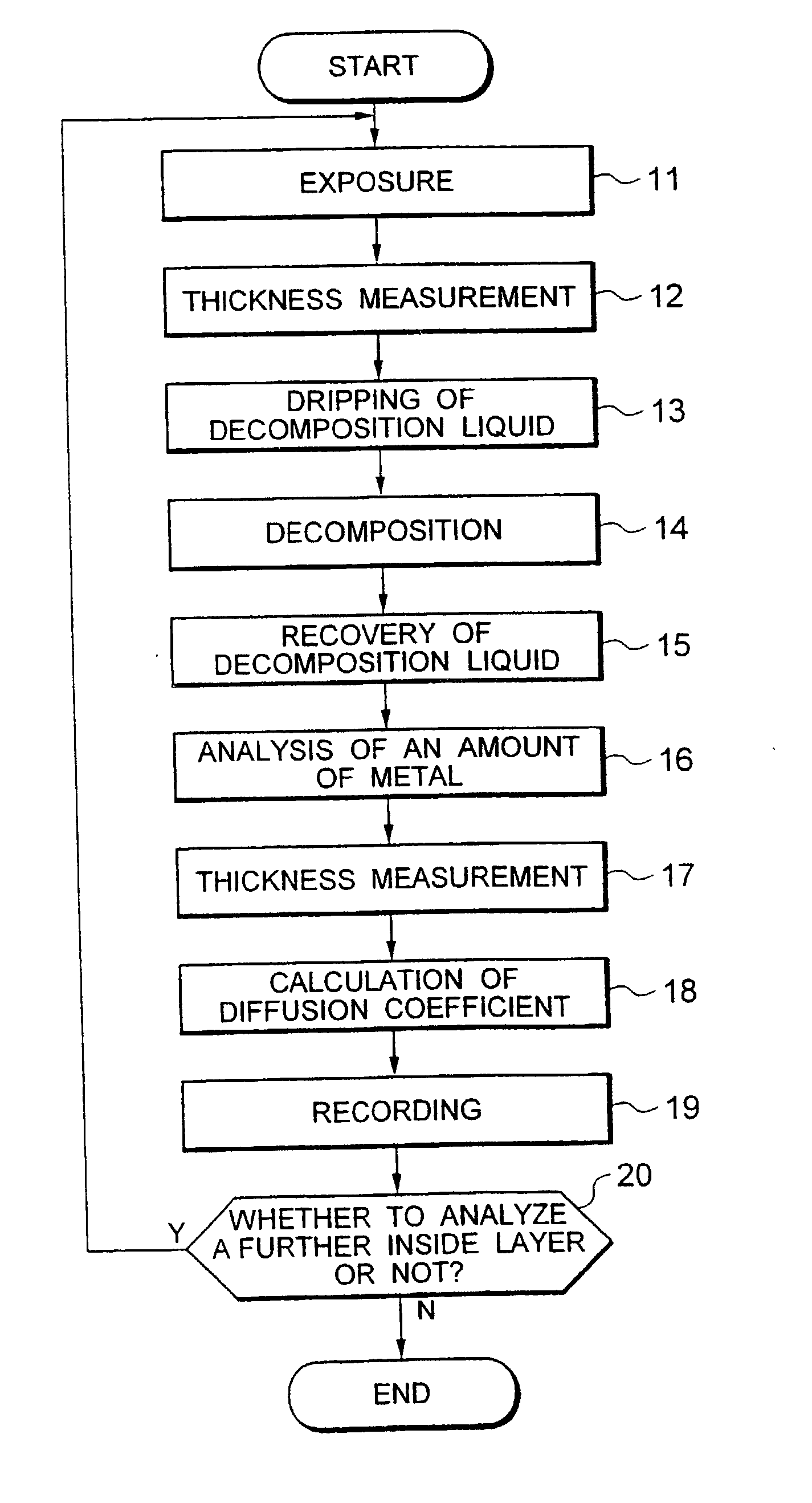
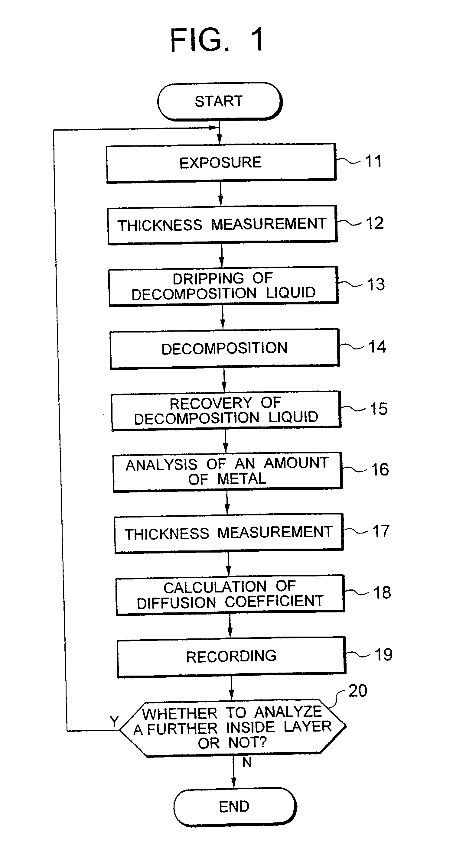
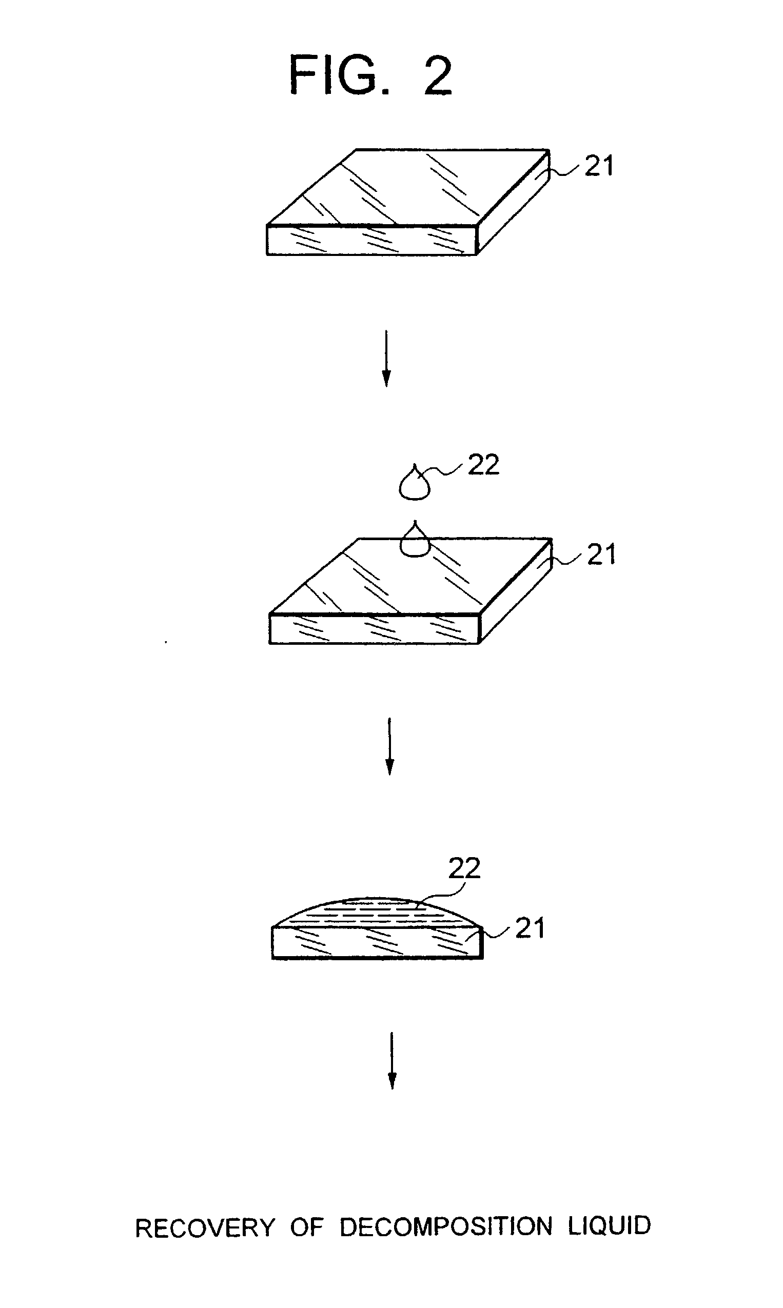
[0061] FIG. 1 is a flowchart showing a flow of an analysis method involving one embodiment, FIG. 2 being a diagram schematically showing circumstances in implementing the above method.

[0062] In implementing an analysis method involving the present invention, first a specimen 21 of for instance rectangle or square is prepared. The specimen 21 is immersed in a surface treatment liquid, hydrofluoric acid (HF) for instance, to etch a surface thereof 21. The etched surface is a surface of a layer to be analyzed. For instance a surface of a layer of a depth of 10 .mu.m from the surface of the specimen 21 is exposed (step 11). At that time, a thickness of a layer to be etched can be controlled by appropriately adjusting the conditions such as a concentration of the treatment liquid such as hydrofluoric acid, an etching period during and a temperature at which the etching is implemented. Furthermore, hydrofluoric acid may be used in any one of liquid and gaseous (va...

example

[0081] In the following, an example of the first embodiment of the present invention will be explained.

[0082] As a specimen for analysis experiment, a quartz specimen for analysis of depth.times.width.times.thickness=20 mm.times.20 mm.times.4 mm was prepared. To investigate a state where copper atoms diffused in the quartz specimen, on a single surface of the specimen a solution of ionized copper of a concentration of 10 .mu.g / g was coated. While maintaining a temperature of 1050.degree. C. under an atmospheric pressure, in this state, the specimen was heated for 24 hours to diffuse copper atoms.

[0083] Next, the specimen, after cleaning the surface thereof, was immersed in hydrofluoric acid. Thereby, the outermost layer of a thickness of approximately 10 .mu.m was etched to expose a surface of a layer necessary to analyze.

[0084] Next, after obtaining a thickness d1 of the specimen, a mixed liquid of 25% hydrofluoric acid and 0.1 N nitric acid was prepared as a decomposition liquid, ...

verification experiment

[0092] (Cross Contamination Verification Experiment)

[0093] Next, a cross contamination verification experiment of the present analysis method was carried out. This will be explained with reference to FIGS. 6A and 6B. For the present experiment, a specimen prepared in the similar way with the aforementioned embodiment (forcedly contaminated specimen 61) and a specimen that is not coated by the copper solution, the quartz specimen as it is (bulk material 62) ware prepared. These two specimens 61 and 62 ware accommodated in the same treatment space 63, with the treatment space 63 under an atmosphere of 50% hydrofluoric acid, being maintained in this state for a definite period.

[0094] The copper concentrations of the respective layers to be analyzed of the forcedly contaminated specimen 61 and bulk material 62 ware analyzed to investigate an influence on the bulk material 62. Here, the copper concentrations of the respective analysis layers ware analyzed for the respective analysis laye...


PUM

PropertyMeasurementUnit
Lengthaaaaaaaaaa
Linear densityaaaaaaaaaa
Dimensionless propertyaaaaaaaaaa

Abstract

Quartz member such as a quartz tube for semiconductor manufacturing equipment capable of heat treating a substrate to be treated without causing contamination, a manufacturing method of such quartz member, thermal treatment equipment furnished with such quartz member, and an analysis method of metal in quartz member are provided. A quartz specimen is immersed in hydrofluoric acid to expose a layer to be analyzed located at a prescribed depth. On an exposed surface, a decomposition liquid such as hydrofluoric acid or nitric acid is dripped to decompose only an extremely thin layer to be analyzed, followed by recovering of the decomposition liquid. The decomposition liquid is quantitatively analyzed by use of atomic absorption spectroscopy (AAS) or the like to measure an amount of metal contained in the decomposition liquid. From a difference of thicknesses before and after the decomposition and an area of dripped decomposition liquid, a volume of a decomposed layer to be analyzed is obtained. From this and the amount of metal contained in the decomposition liquid, a concentration of metal contained in the layer to be analyzed, in addition a diffusion coefficient of a layer to be analyzed is calculated. With thus obtained diffusion coefficient as an index, quartz material in which metal diffuses with difficulty is sorted out. With thus sorted quartz material, a quartz member used for semiconductor manufacturing equipment such as a quartz tube is manufactured.

Description

[0001] The present invention relates to quartz member for semiconductor manufacturing equipment, a manufacturing method of quartz member for semiconductor manufacturing equipment, thermal treatment equipment, and an analysis method of metal in quartz member. In particular, the present invention relates to quartz member for semiconductor manufacturing equipment suitable for heat treating semiconductor substrates such as silicon wafers, a manufacturing method of quartz member for semiconductor manufacturing equipment, thermal treatment equipment and a method for analyzing metal in quartz member.PRIOR ART[0002] Thermal treatment equipment for heat treating semiconductor wafers accommodates therein a plurality of pieces of semiconductor wafers held in an approximately level state in thermal treatment equipment to heat by means of a heater. FIG. 12 is a vertical sectional view showing a rough configuration of typical thermal treatment equipment.[0003] As shown in FIG. 12, a plurality of ...

Claims


Application Information

Patent Timeline
IPC IPC(8): C03B20/00G01N27/62C03C15/00C30B31/10C30B35/00G01N1/32G01N1/34G01N1/40G01N19/06G01N21/31G01N21/73
CPCC30B31/10C30B35/00Y10T117/10G01N1/4044G01N1/32H01L21/324
Inventor MARUMO, YOSHINORISUZUKI, KANAMEHAYASHI, TERUYUKITANAHASHI, TAKASHI
Owner TOKYO ELECTRON LTD
Learn More