Method of plasma etching doped polysilicon layers with uniform etch rates

a technology of arsenic doped polysilicon and plasma etching, which is applied in the direction of basic electric elements, semiconductor/solid-state device manufacturing, electrical equipment, etc., can solve the problems of poor uniformity of first sub-etch steps within the same wafer, non-functional memory cells, and poor uniformity of first sub-etch steps, etc., to achieve accurate control, and high level of thickness uniformity

Inactive Publication Date: 2001-05-24
IBM CORP
View PDF0 Cites 15 Cited by
  • Summary
  • Abstract
  • Description
  • Claims
  • Application Information

AI Technical Summary

Benefits of technology

0019] It is another object of the present invention to provide a method of forming an arsenic doped polysilicon strap in an opening of a patterned BPSG layer by plasma etching with a high level of thickness uniformity within a wafer.
0020] It is still another object of the present invention to provide a method of forming an arsenic doped polysilicon strap in an opening of a patterned BPSG layer by plasma etching wherein the completion of the plasma etching process is very accurately and securely controlled by an optical etch end point system.
0021] The accomplishment of these and other related objects is achieved by the method of the present invention which aims to get rid of these drawbacks. According to the method of the present invention, there is disclosed a combination of both system and process improvements that allow plasma etching of an arsenic doped polysilicon layer formed over a patterned layer of a dielectric such as BPSG with an uniform etch rate. The system improvement consists to hold the wafer during the etch process with an elec...

Problems solved by technology

Unfortunately, the first sub-etch step has a very poor uniformity within a same wafer, typically 10% at one sigma.
As far as "empty" straps are concerned, it is clear that the strap integrity is jeopardized.
"Empty straps" cause so-called "OPEN" contacts, i.e. no electrical contact is possible between the capacitor top electrode and the IGFET drain reg...

Method used


Image

  • Method of plasma etching doped polysilicon layers with uniform etch rates
  • Method of plasma etching doped polysilicon layers with uniform etch rates
  • Method of plasma etching doped polysilicon layers with uniform etch rates

Examples


Embodiment Construction

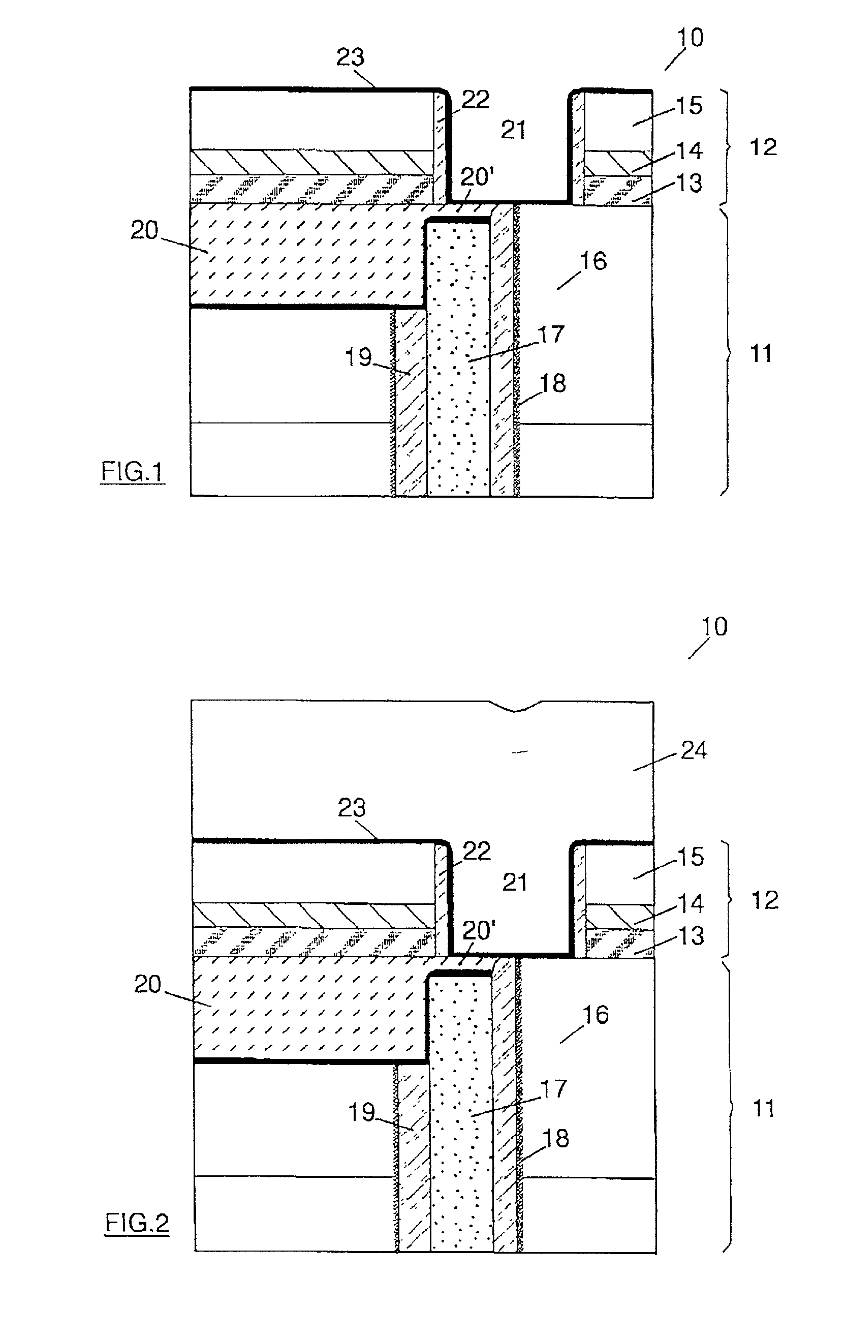
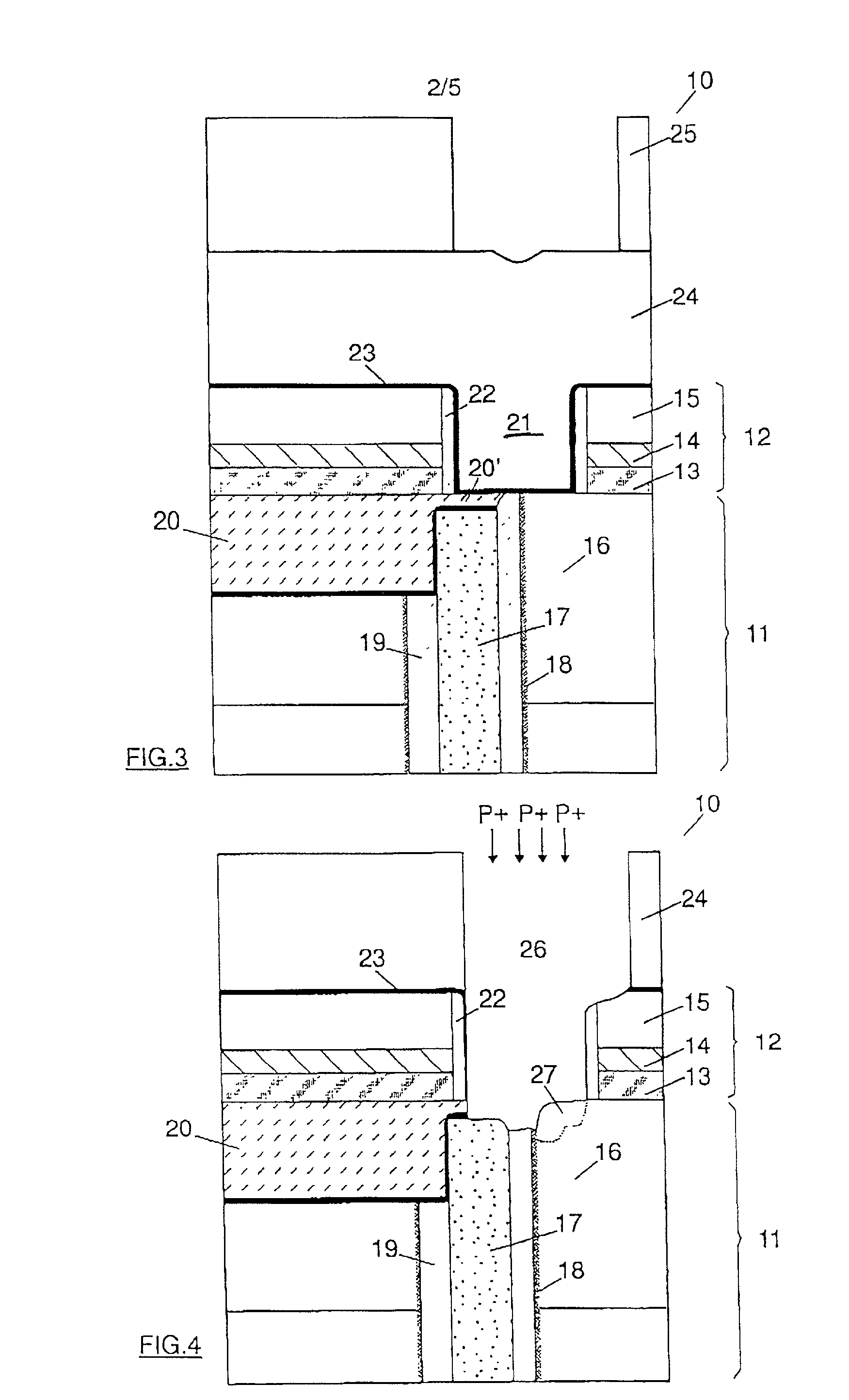
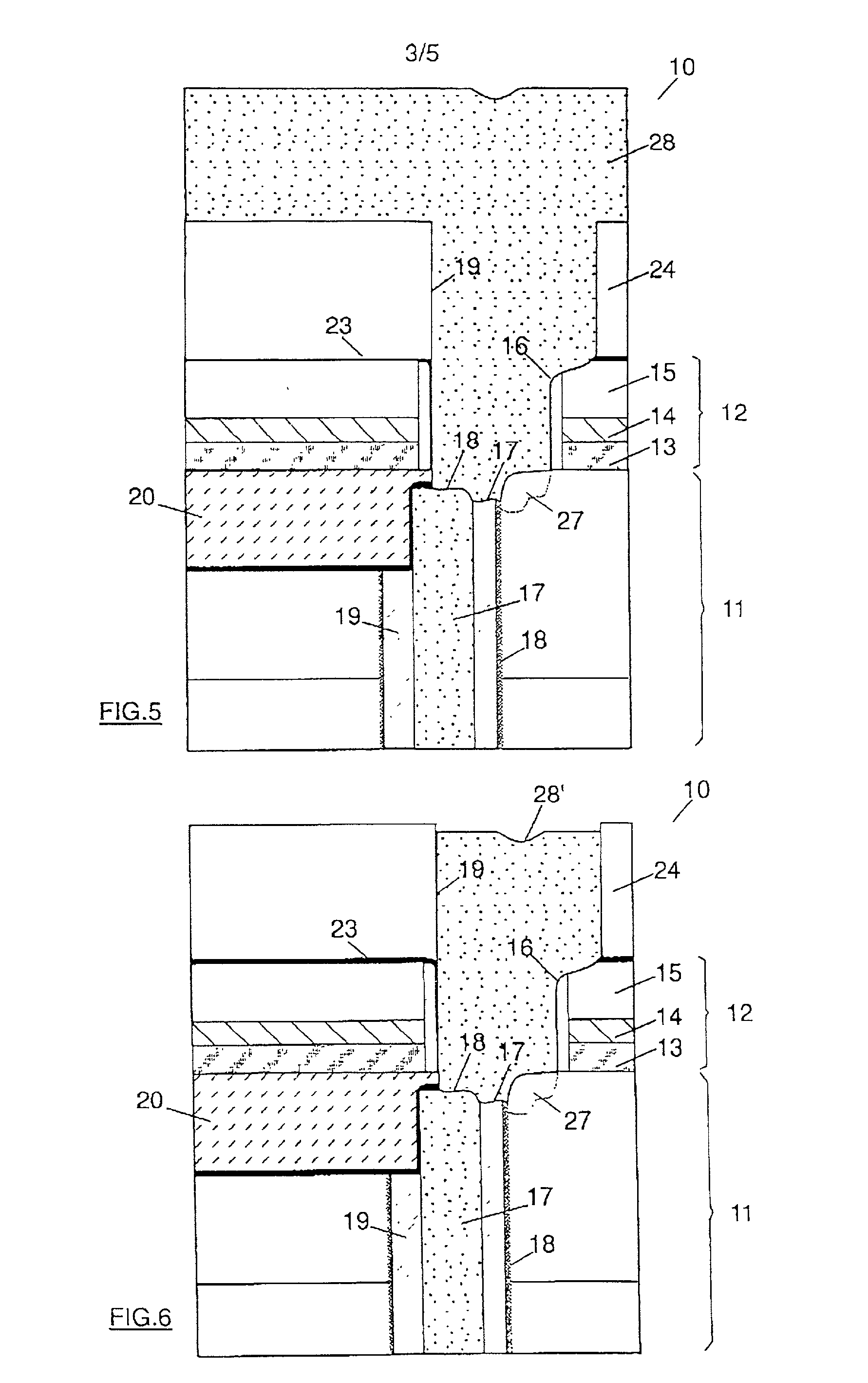
[0027] Applicant's inventors have discovered that the plasma etching process of the prior art could be significantly improved only if both the wafer plasma environment and the etching chemistry were changed during the first sub-etch step.

[0028] Firstly, the etching of the doped polysilicon layer must be conducted with a plasma that is perfectly uniform all over the wafer surface and this can be obtained only if the wafer is placed on an electrostatic chuck device (ECD). Electrostatic wafer holding has become very desirable in the vacuum handling and processing of semiconductor wafers for a number of reasons. However, the specific feature which is important here is only the absence of clamps (or grippers) that are of general use on the other types of wafer holders. The absence of clamps has been appreciated so far as a source of contamination reduction. Without clamps, less cracks are produced in the wafer during the handling and processing operations. As a result, it has been notice...


PUM


Abstract

In wafer semiconductor manufacture, a method of etching an arsenic doped polysilicon layer down to a patterned boro-phospho-silicate-glass (BPSG) layer provided with a plurality of openings with an uniform etch rate is disclosed. The method relies on a combination of both system and process improvements. The system improvement consists to hold the wafer in the reactor during the etch process with an electrostatic chuck device to have a perfect plasma environment around and above the wafer. On the other hand, the process improvement consists in the use of a non dopant sensitive and not selective chemistry. A NF3/CHF3/N2 gas mixture with a 11/8.6/80.4 ratio in percent is adequate in that respect. The etch time duration is very accurately controlled by an optical etch endpoint detection system adapted to detect the intensity signal transition of a CO line at the BPSG layer exposure. The process is continued by a slight overetching. When the above method is applied to the doped polysilicon strap formation in DRAM chips, excessive or insufficient etching of the polysilicon layer is avoided, so that the doped polysilicon strap thickness is thus much more uniform, opening to opening, within a wafer.

Description

[0001] The present invention relates to the manufacture of semiconductor integrated circuits (ICs) and more particularly to a method of plasma etching a doped polysilicon layer formed on a patterned dielectric layer with an uniform etch rate. The method finds a very useful application in forming doped polysilicon straps in a boro-phospho-silicate glass (BPSG) layer provided with strap openings with a high level of thickness uniformity in DRAM chips.[0002] In the manufacture of semiconductor integrated circuits, and particularly in Dynamic Random Access Memory (DRAM) chips, polysilicon straps are extensively used. In DRAM chips, an Insulated Gate Field Effect Transistor (IGFET) and a storage capacitor associated thereto form the elementary memory cell. Polysilicon straps are built between the drain region of the IGFET transistor and an electrode of the capacitor to allow an electrical contact therebetween.[0003] The essential steps of a conventional polysilicon strap (PS) formation p...

Claims


Application Information

Patent Timeline
IPC IPC(8): H01L21/3213H01L21/768
CPCH01L21/32137H01L21/76838H01L21/3065
Inventor LEVERD, FRANCOLSMACCAGNAN, RENZOMASS, ERIC
Owner IBM CORP
Why Eureka
Try Eureka