Light escalators in optical circuits between thick and thin waveguides

a waveguide and waveguide technology, applied in the field of photonic circuits, can solve the problems of large power consumption, difficult and costly integration with silicon photonics, and large device volume, and achieve the effects of low capacitance of vertical contacts, small detector volume, and high speed

Active Publication Date: 2021-11-16
TEKNOLOGIAN TUTKIMUSKESKUS VTT
View PDF13 Cites 3 Cited by
  • Summary
  • Abstract
  • Description
  • Claims
  • Application Information

AI Technical Summary

Benefits of technology

[0042]The invention offers considerable benefits. In the case of detectors only a thin layer of Ge is needed, instead of the 3 μm thick Ge layer usually needed to make a detector on a 3 μm thick SOI. In this way the detector volume can be small and capacitance of vertical contacts can be low, paving the way to high speed devices. Also, unlike a 3 μm thick germanium layer grown on etched silicon, in the present invention Ge may be grown on high quality non-etched silicon surface, which makes the quality of the material much higher, with positive impact on sensitivity and dark current. Further, contacts for the devices can be implanted directly on flat a thick silicon surface. Similarly, a thin layer of SiGe alloy with suitable bandgap can be deposited to realize fast Franz-Keldysh modulators with smaller volume than existing devices in microscale silicon platforms. 2D materials, such as graphene, can be easily integrated and sandwiched between waveguides of amorphous and crystalline silicon, with suitable dielectric insulating layers.

Problems solved by technology

They often have to be made of different materials that are difficult and costly to integrate with silicon photonics.
The problem to be solved is how to structure and fabricate graphene modulators on thick SOI waveguides, so that the graphene is interacting with the optical field.
Photonics circuits based on micron-scale (3 μm thick) silicon-on-insulator (SOI) waveguides have many advantages compared to standard submicron (220 nm-400 nm thick) silicon waveguide technology, but also some major limitations.
Namely larger waveguide size implies devices with larger power consumption and, even more importantly, slower speed.
This makes this thicker platform less attractive compared to others for most applications requiring high speed modulation and detection.
Prior art solutions to the problem include the use of submicron silicon waveguides for the whole circuit, which comes with many drawbacks, including high propagation losses, single-polarization operation, bad tolerances to fabrication errors, not to mention the requirement for very expensive deep UV fabrication tools.
Fast devices have been demonstrated on thick SOI waveguides, where the volume of the devices was reduced by patterning sub-micron wide waveguides with a high aspect ratio, which makes the fabrication challenging and with a bad impact on yield.

Method used


Image

  • Light escalators in optical circuits between thick and thin waveguides
  • Light escalators in optical circuits between thick and thin waveguides
  • Light escalators in optical circuits between thick and thin waveguides

Examples


Embodiment Construction

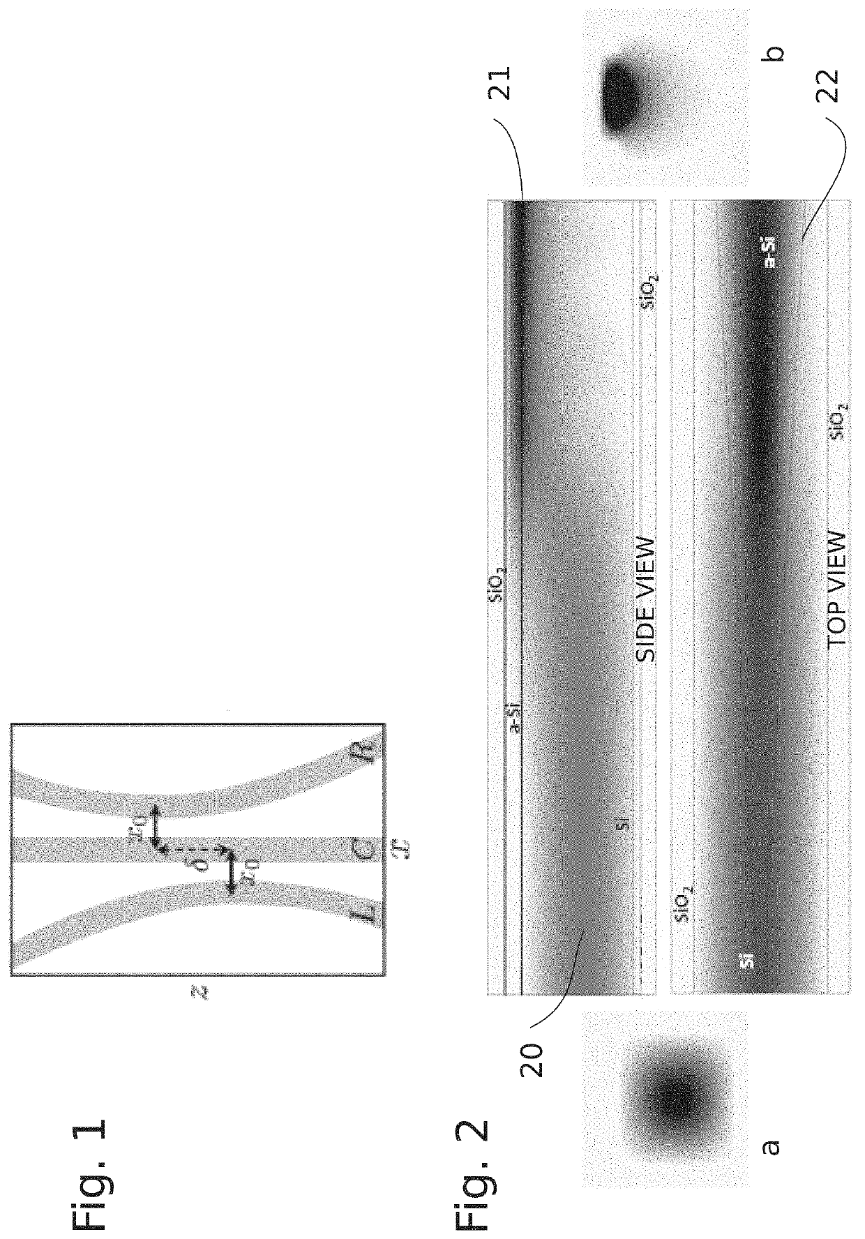
[0062]FIG. 1 illustrate the phenomenon of adiabatic light transfer. In FIG. 1 is shown a schematic top view a system of three waveguides consisting of two circularly bent outermost waveguides L and R, and one straight central waveguide C. The minimum distance between waveguides is given by x0, and the z distance between the centers of the curved waveguides is defined by δ. The radius of curvature of the outermost waveguides L, R may be is 3.5 m, the spatial delay δ=4200 μm, for example, and the minimum separation between waveguides x0=7 μm, for example.

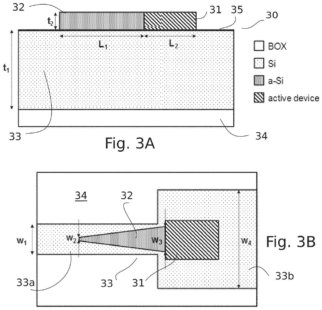
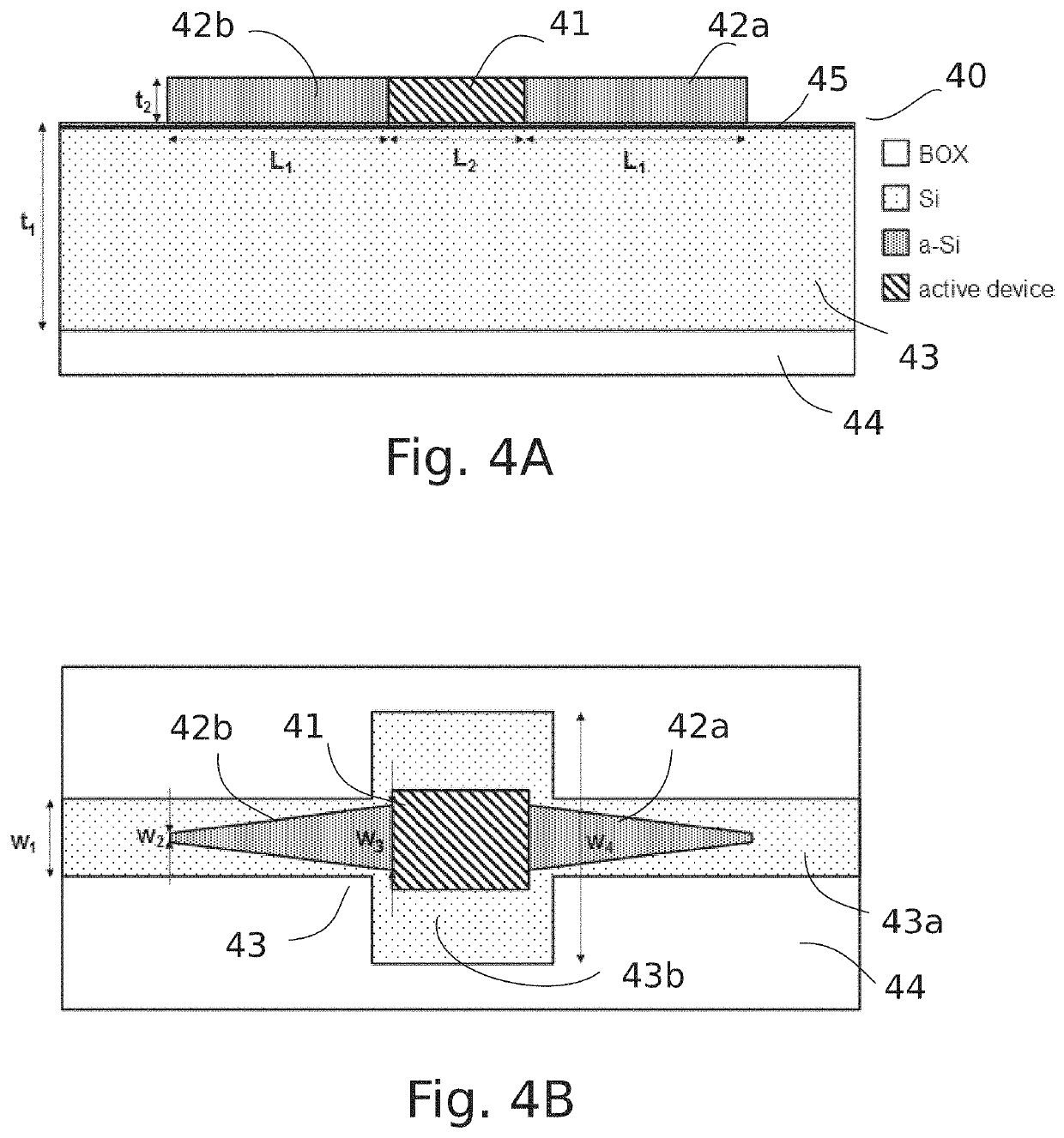
[0063]FIG. 2 shows a side view and a top view of an exemplary inventive waveguide, where a simulation shows how the light is transferred from a lower thick silicon waveguide 20 made of crystalline silicon Si to an upper tapered (22) and thin hydrogenated amorphous silicon (a-Si:H) waveguide 21, with a refractive index higher than that of crystalline silicon. The cross-section “a” to the left further illustrate the light distribution a...


PUM

PropertyMeasurementUnit
thicknessaaaaaaaaaa
thicknessaaaaaaaaaa
thickaaaaaaaaaa

Abstract

The invention relates to photonic circuits, in particular to photonic circuits where light is escalated transferred between optical waveguides which are coupled to photonic devices. A first waveguide on a silicon substrate is provided having a first thickness and a first refractive index. A tapered second waveguide having a second thickness less than the first thickness and a second refractive index higher than said first refractive index is deposited on the first waveguide. At least one layer of an optically active material comprising a photonic device is deposited on the first waveguide adjacent to the second waveguide. The photonic device is interfaced with the wide end of the tapered second waveguide to provide an optical coupling, and the opposite narrow end of the tapered second waveguide is interfaced on top of the first waveguide to provide adiabatic light transfer between said first and second waveguides.

Description

FIELD OF THE INVENTION[0001]The invention relates to photonic circuits and their manufacture, in particular to photonic circuits where light is transferred between optical waveguides, which are coupled to photonic devices.BACKGROUND OF THE INVENTION[0002]Optical communication systems are continuously being miniaturized to integrate a large number of previously discrete optoelectronic devices with silicon-based integrated circuits to achieve on-chip optical interconnects for high performance computation. In particular, silicon photonics aims to integrate as many as possible optoelectronic functionalities based on CMOS compatible materials, in order to lower the cost without sacrificing performance.[0003]Optical modulators and photodetectors are main building blocks of photonic systems. These two types of devices operate based on very different mechanisms and consequently utilize different device geometries. They often have to be made of different materials that are difficult and cost...

Claims


Application Information

Patent Timeline
Patent Type & Authority Patents(United States)
IPC IPC(8): G02B6/122G02B6/12
CPCG02B6/1228G02B2006/12061G02B2006/12138G02B2006/12142G02B2006/12147G02B6/14G02B2006/12152G02B6/12002G02B6/12004G02F1/025
Inventor CHERCHI, MATTEOAALTO, TIMOARPIAINEN, SANNA
Owner TEKNOLOGIAN TUTKIMUSKESKUS VTT
Why Eureka
Try Eureka