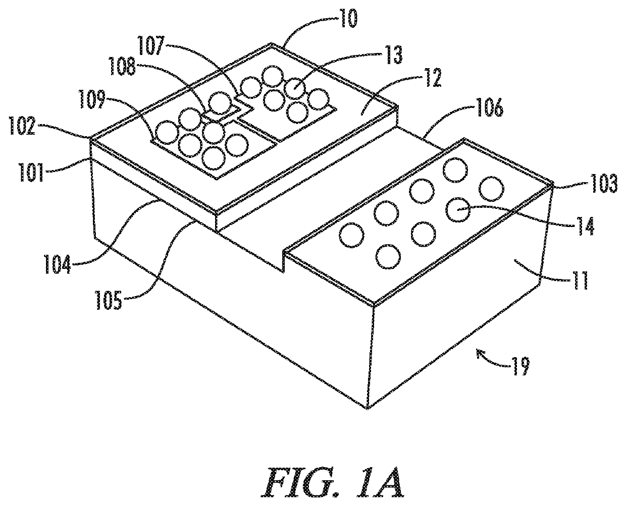
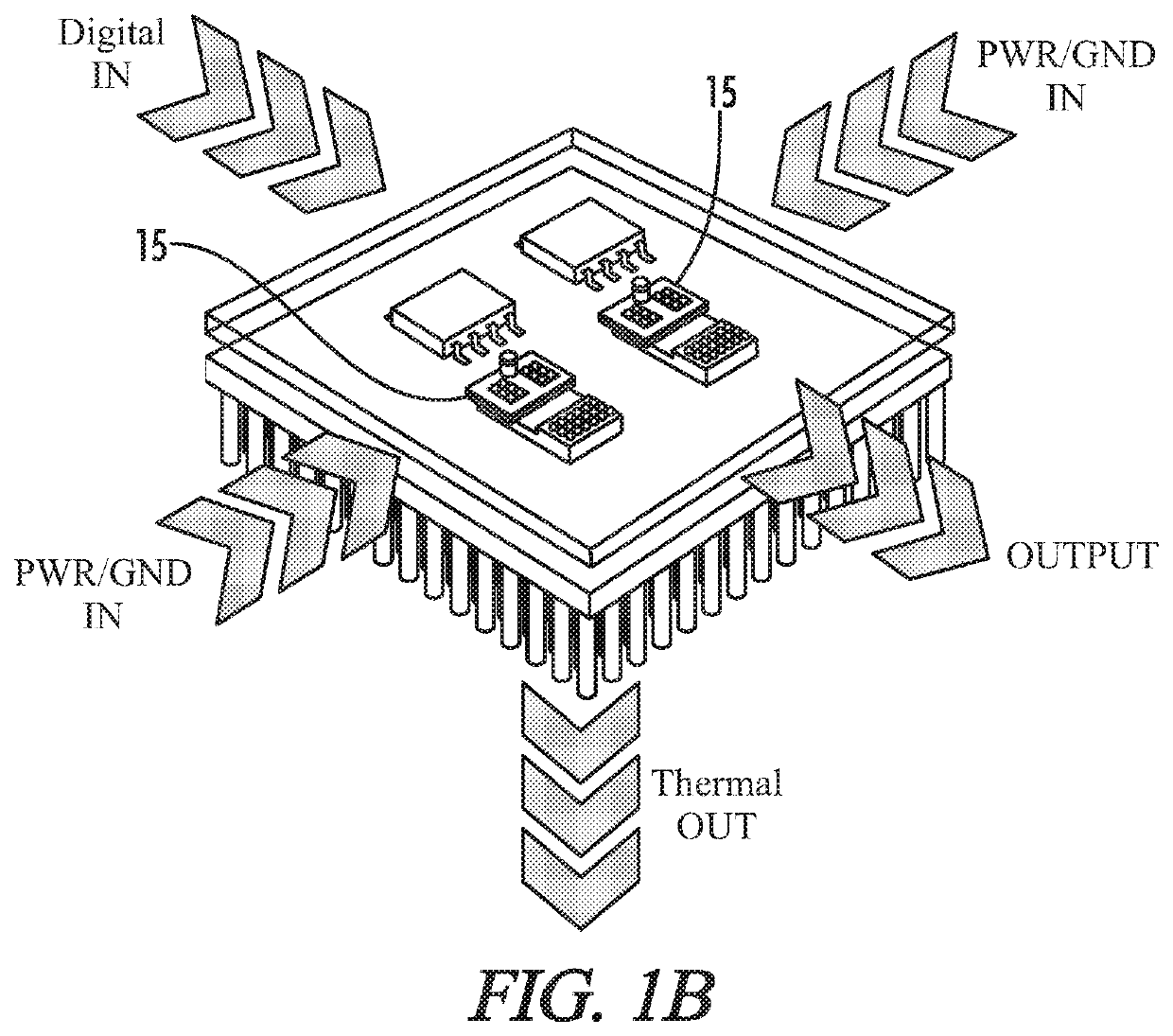
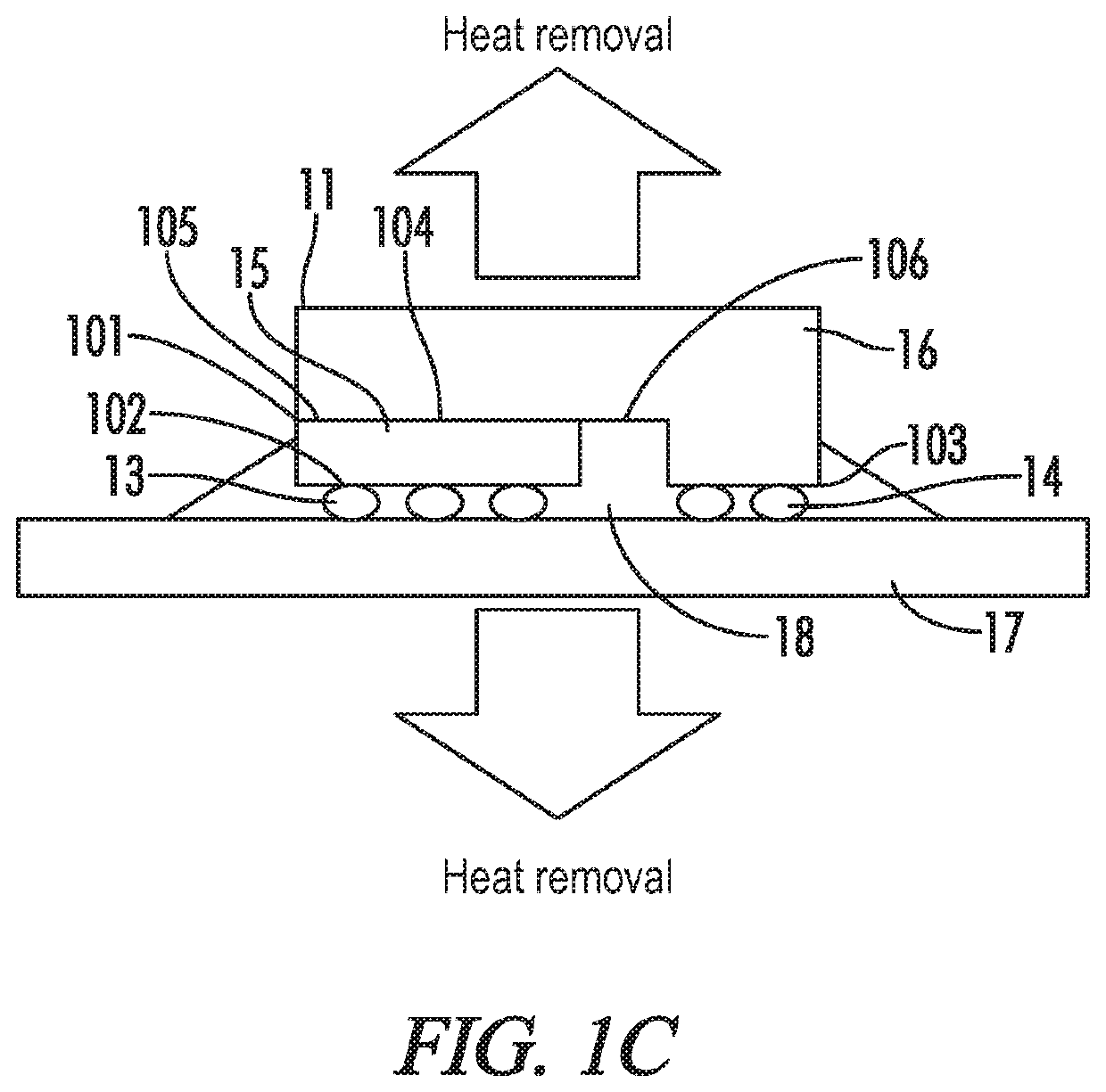
Flip-chip wire bondless power device
a power device and flip-chip technology, applied in semiconductor devices, semiconductor/solid-state device details, electrical apparatus, etc., can solve the problems of wire bonded modules not being able to achieve 3d architectures and double-sided cooling schemes, and the risk of reliability, etc., to achieve simple and economical manufacturing processes and high power density.
- Summary
- Abstract
- Description
- Claims
- Application Information
AI Technical Summary
Benefits of technology
Problems solved by technology
Method used
Image

Examples
example
[0085]The following example provides a detailed account of the manufacturing process and electrical testing of a preferred embodiment of the invention. First the process of fabricating a flip-chip MOSFET package, starting from a commercial off the shelf bare die power device is described following by a description of a test setup and test results of the fabricate samples.
[0086]In the first step of this example, the re-metallization of the top side contact of bare power devices were performed as shown in FIG. 4. Prior to mounting, the samples were rinsed thoroughly in isopropyl alcohol and dried in step 40. The bare die power devices were mounted on 1″×1″ alumina plates using double sided Kapton tape in step 41. The mounted samples were cleaned a second time for five minutes in an argon plasma in step 42a. A third cleaning cycle was conducted using an alkaline etch cleaner, MCL-16, purchased from UYEMURA, 3990 Concours, #425 Ontario, CA 91764 in step 42b. The sample was then subjecte...
PUM
 Abstract
Description
Claims
Application Information
 - R&D
- Intellectual Property
- Life Sciences
- Materials
- Tech Scout
- Unparalleled Data Quality
- Higher Quality Content
- 60% Fewer Hallucinations
Browse by: Latest US Patents, China's latest patents, Technical Efficacy Thesaurus, Application Domain, Technology Topic, Popular Technical Reports.
© 2025 PatSnap. All rights reserved.Legal|Privacy policy|Modern Slavery Act Transparency Statement|Sitemap|About US| Contact US: help@patsnap.com