
Crystalline oxide semiconductor thin film, method for producing crystalline oxide semiconductor thin film, and thin film transistor

a technology of crystalline oxide semiconductor and thin film transistor, which is applied in the direction of vacuum evaporation coating, polycrystalline material growth, crystal growth process, etc., can solve the problems that the variability of tft characteristics cannot be suppressed and new measures have become necessary, and achieve the effect of lowering the mobility

Active Publication Date: 2020-04-28
IDEMITSU KOSAN CO LTD
View PDF33 Cites 0 Cited by
  • Summary
  • Abstract
  • Description
  • Claims
  • Application Information

AI Technical Summary

Benefits of technology

[0018]In addition, in order to enhance the mobility and reliability of the oxide semiconductor film for a display, it is important to reduce traps existing in the energy gap of the oxide semiconductor. As one of methods for reducing traps, a method is given in which water is introduced into the chamber during sputtering to oxidize more effectively (for example, Patent Document 8). Water is decomposed in plasma, and becomes an OH radical that shows an extremely strong oxidizing power, thus exhibiting effects of reducing traps in an oxide semiconductor. However, a process of introducing water requires removal of oxygen and nitrogen dissolved in water sufficiently in advance. In addition, there is a problem that new measures have become necessary such as prevention of corrosion of a piping.
[0020]An object of the invention is to provide a crystalline oxide semiconductor thin film having a stable carrier density and a thin film transistor having a high saturation mobility when this film is used as a channel layer of a thin film transistor.
[0021]Under such circumstances, the inventors formed an oxide thin film formed mainly of indium oxide without introducing impurities such as water, and heated, whereby a crystalline oxide semiconductor thin film containing surface crystal grains having a single crystal orientation was obtained. The inventors also found that, by allowing the crystal state of the oxide thin film to be in the above-mentioned state, the crystal is stabilized, whereby variations in carrier density of an oxide thin film can be suppressed, and as a result, variations in TFT characteristics can be suppressed.
[0046]According to the invention, it is possible to provide a crystalline oxide semiconductor thin film having a stable carrier density and a thin film transistor having a high saturation mobility obtained by using the same.

Problems solved by technology

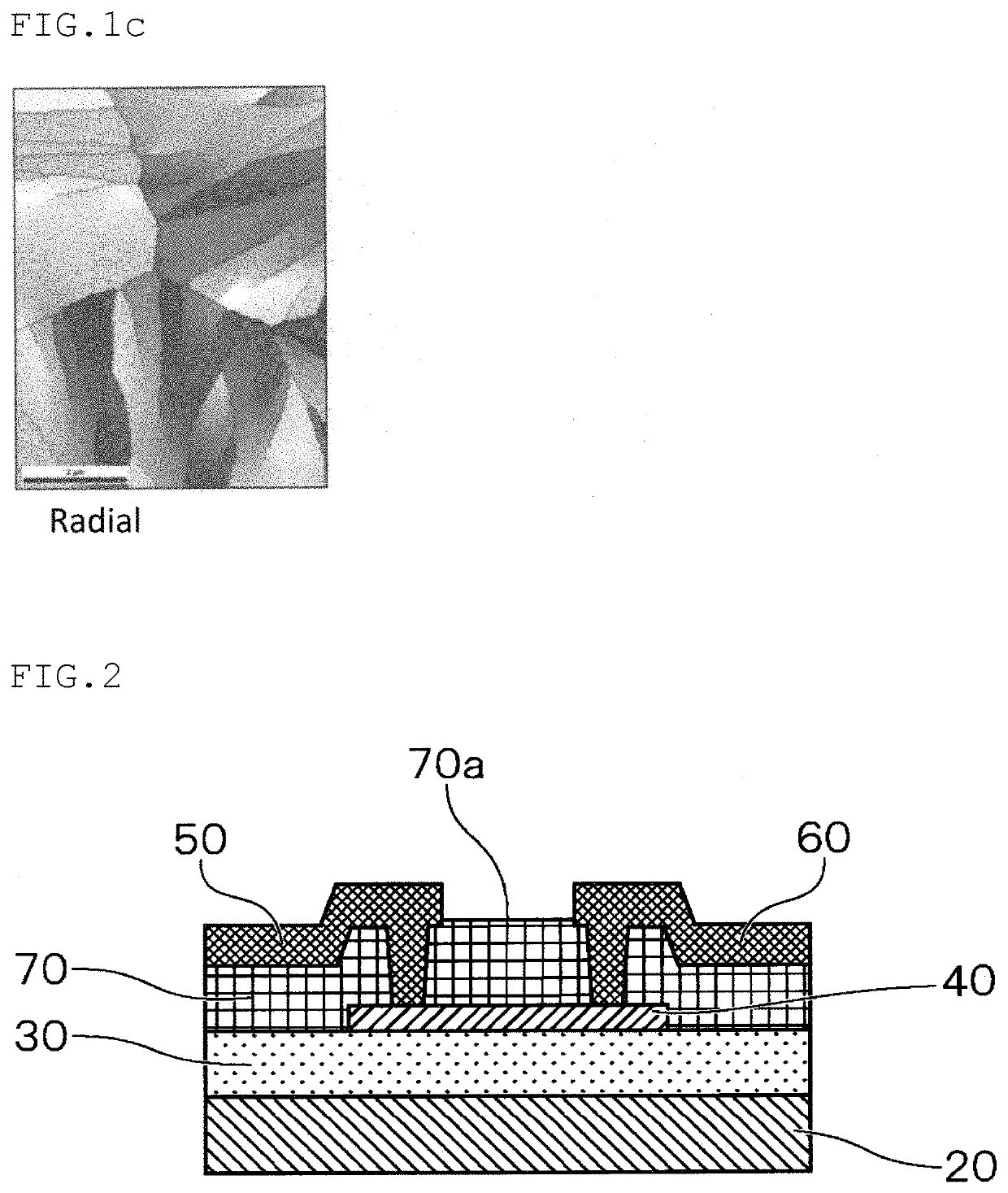
For example, when an oxide thin film is crystallized by heating at a rapid temperature-elevation speed, crystal growth occurs radially, whereby the crystal orientation becomes radial, and a large number of lattice defects causing the carrier density variation are formed in the inside of a crystal grain.
Therefore, in a crystalline oxide semiconductor thin film, there is a still problem that the carrier density is varied, and hence variations in TFT characteristics cannot be suppressed.
In addition, there is a problem that new measures have become necessary such as prevention of corrosion of a piping.

Method used


Image

  • Crystalline oxide semiconductor thin film, method for producing crystalline oxide semiconductor thin film, and thin film transistor
  • Crystalline oxide semiconductor thin film, method for producing crystalline oxide semiconductor thin film, and thin film transistor

Examples


example 1

[0096]The thin film transistor having a structure shown in FIG. 2 was produced by the following steps:

(1) Film-Forming Step

[0097]By sputtering using a sputtering target obtained by mixing 96 wt % (89.8 at %) of indium oxide and 4 wt % (10.2 at %) of aluminum oxide, on a silicon wafer (gate electrode 20) with a thermally oxidized film (gate insulating film 30), a 50 nm-thick thin film (oxide semiconductor layer 40) was formed through a metal mask. As the sputtering gas, a mixed gas of high-purity argon and high-purity oxygen (concentration of impurities: 0.01 vol %) was used, and sputtering was conducted under the film-forming conditions shown in Table 1-1.

(2) Heating Step

[0098]The obtained stacked body was subjected to a heat treatment in the air at the temperature, the time and the conditions shown in Table 1-1. The “heat treatment after film formation: time (min)” in the “heat treatment conditions after the formation of the semiconductor film” in Table 1-1 means the time taken fro...

examples 10 and 11

[0127]Thin film transistors were produced in the same manner as in Example 1, except that semiconductor thin films were formed by using the sputtering targets having compositions shown in Table 2 and a heat treatment or the like were conducted, and properties of a TFT were evaluated.

[0128]Further, in the same manner as in Example 1, for a sample on which only an oxide thin film was mounted on a glass substrate, hall measurements were conducted at each stage in Table 2. An increase or decrease in carrier density and band gap were measured, and the results are shown in Table 2.

[0129]In the atomic ratio of the sputtering targets shown in the table, the numerical value shown by the “wt %” indicates the weight ratio (charged amount) of indium oxide, gallium oxide, yttrium oxide and tin oxide, the numerical value indicated by the “at %” indicates an indium element, a gallium element, an yttrium element and a tin element.

[0130]The “E+XX” in the table means “1×10+XX”.

[0131]The “ratio of the...

examples 12 and 13

[0133]Thin film transistors were produced in the same manner as in Example 1, except that semiconductor thin films were formed by using sputtering targets having the compositions shown in Table 3 and a heat treatment or the like were conducted, and properties of a TFT were evaluated.

[0134]In the same manner as in Example 1, for a sample on which only an oxide thin film was mounted on a glass substrate, hall measurement was conducted at each stage shown in Table 3, and an increase or decrease of carrier density and band gap were measured. The results are shown in Table 3.

[0135]In the atomic ratio of the sputtering target in the table, the numerical value indicated by “wt %” shows the weight ratio (charged amount) of indium oxide, gallium oxide, samarium oxide and tin oxide, and the numerical value indicated by “at %” shows the atomic value of an indium element, a gallium element, a samarium element and a tin element.

[0136]The “E+XX” in the table means “1×10+XX”.

[0137]The “ratio of th...


PUM

PropertyMeasurementUnit
average crystal diameteraaaaaaaaaa
band gapaaaaaaaaaa
temperatureaaaaaaaaaa

Abstract

A crystalline oxide semiconductor thin film that is composed mainly of indium oxide and comprises surface crystal grains having a single crystal orientation.

Description

CROSS-REFERENCE TO RELATED APPLICATIONS[0001]The present application is a U.S. national stage application claiming the benefit of International Patent Application No. PCT / JP2016 / 003528, filed Jul. 29, 2016, which claims the benefit of priority to Japanese Patent Application No. 2015-150701, filed Jul. 30, 2015, the entireties of which are hereby incorporated by reference.TECHNICAL FIELD[0002]The invention relates to a crystalline oxide semiconductor thin film. In particular, the invention relates to a crystalline oxide semiconductor thin film of a thin film transistor (TFT) used in a display such as a liquid crystal display or an organic EL display. The crystalline oxide semiconductor thin film of the invention can be preferably used in a solar cell, a display such as a liquid crystal element, an organic electroluminescence element and an inorganic electroluminescence element, and an electronic device such as a power semiconductor device and a touch panel. These can be preferably us...

Claims


Application Information

Patent Timeline
Patent Type & Authority Patents(United States)
IPC IPC(8): H01L29/786H01L29/24H01L29/66H01L29/04C30B29/16C30B1/02C23C14/58C23C14/34C23C14/08C01G15/00H01L21/02
CPCH01L29/24C23C14/5806H01L21/02592H01L21/02595C01G15/00C23C14/34C23C14/08C23C14/086H01L29/04H01L21/02667H01L21/02565H01L29/7869H01L29/66969C30B29/16C30B1/023H01L21/02631C01P2006/40C01P2004/61C01P2002/70C01P2002/54H01L29/78618H01L29/78603H01L21/324
Inventor INOUE, KAZUYOSHIUTSUNO, FUTOSHITSURUMA, YUKITOMAI, SHIGEKAZUEBATA, KAZUAKI
Owner IDEMITSU KOSAN CO LTD
Learn More