Manufacture method of amoled pixel drive circuit
- Summary
- Abstract
- Description
- Claims
- Application Information
AI Technical Summary
Benefits of technology
Problems solved by technology
Method used
Image
Examples
Embodiment Construction
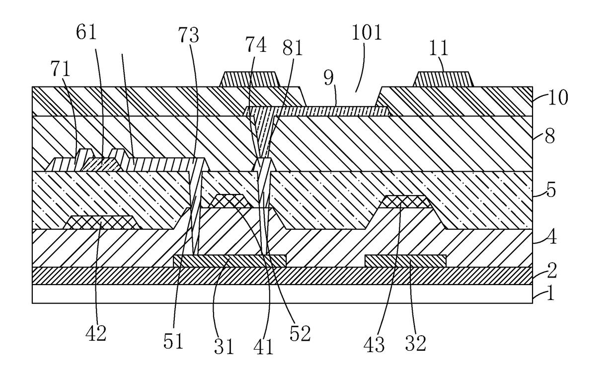
[0059]For better explaining the technical solution and the effect of the present invention, the present invention will be further described in detail with the accompanying drawings and the specific embodiments.
[0060]Please refer to FIG. 11. The present invention provides a manufacture method of an AMOLED pixel driving circuit, comprising steps of:
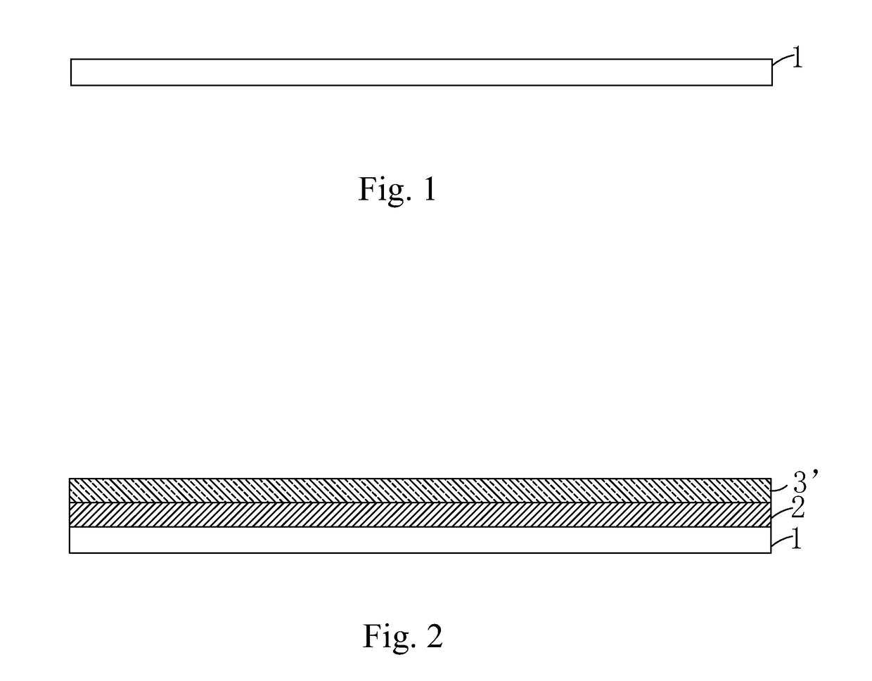
[0061]step 1, referring to FIG. 1, providing a substrate 1, and performing clean and pre-cure to the substrate 1.
[0062]Specifically, the substrate 1 is a transparent substrate and preferably to be a glass substrate.
[0063]step 2, referring to FIG. 2, depositing a buffer layer 2 on the substrate 1, and depositing an amorphous silicon layer 3′ on the buffer layer 2.
[0064]Specifically, material of the buffer layer 2 is one or more combinations of silicon oxide (SiOx) and silicon nitride (SiNx).
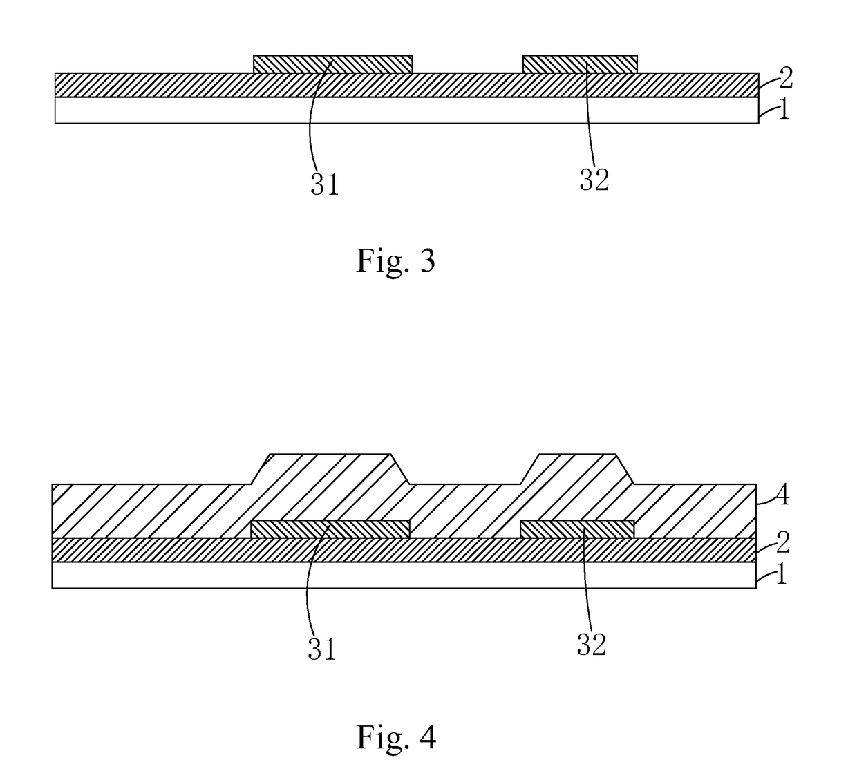
[0065]step 3, referring to FIG. 3, performing P type ion doping and rapid thermal annealing (RTA) to the amorphous silicon layer 3′ to crystallize the sa...
PUM
 Abstract
Description
Claims
Application Information
 - R&D
- Intellectual Property
- Life Sciences
- Materials
- Tech Scout
- Unparalleled Data Quality
- Higher Quality Content
- 60% Fewer Hallucinations
Browse by: Latest US Patents, China's latest patents, Technical Efficacy Thesaurus, Application Domain, Technology Topic, Popular Technical Reports.
© 2025 PatSnap. All rights reserved.Legal|Privacy policy|Modern Slavery Act Transparency Statement|Sitemap|About US| Contact US: help@patsnap.com


