
C12A7 electride thin film fabrication method and C12A7 electride thin film

a technology of electride and thin film, which is applied in the direction of oxide conductors, non-metal conductors, vacuum evaporation coatings, etc., can solve the problems of inconvenient method for fabricating a crystalline c12a7 electride thin film, the combination of materials that may be used for the thin film and the substrate may be very limited, and the heat resistance of materials that may be used as the substrate may be limited

Active Publication Date: 2019-04-02
AGC INC +1
View PDF23 Cites 0 Cited by
  • Summary
  • Abstract
  • Description
  • Claims
  • Application Information

AI Technical Summary

Benefits of technology

[0008]Crystalline C12A7 having such conductive properties is referred to as a crystalline C12A7 electride. Because crystalline C12A7 electrides have a very low work function of about 2.4 eV, advantageous effects can be expected by applying crystalline C12A7 electrides to electron injection electrodes of organic EL (electroluminescence) elements and cold electron emission sources, or reducing agents used in chemical reactions, for example.
[0009]Generally, a crystalline C12A7 bulk is fabricated by performing a sintering process on crystalline C12A7 electride powder under a high-temperature reducing atmosphere (Patent Document 1). For example, the temperature of the sintering process may be about 1200° C.
[0010]Although the above conventional method may be effective for fabricating the crystalline C12A7 in bulk, the method is not suitable for fabricating a crystalline C12A7 electride thin film.
[0011]That is, in the case of fabricating a crystalline C12A7 electride thin film using a conventional method requiring a high temperature of about 1200° C., for example, materials that may be used as the substrate of the thin film may be limited to heat resistant materials. As a result, the combination of the types of materials that may be used for the thin film and the substrate may be very limited.
[0012]For example, a glass substrate is often used as a versatile substrate for various types of electrical devices and elements. However, the temperature limit for a glass substrate is about 700° C. at most. Accordingly, it would be difficult to form a crystalline C12A7 electride thin film on a glass substrate using a conventional fabrication method owing to the temperature limit of the glass substrate.
[0013]In light of the above, there is a growing demand for a technique for fabricating a C12A7 electride thin film under a low processing temperature to avoid or alleviate the above-described shortcomings.SUMMARY OF THE INVENTION

Problems solved by technology

Although the above conventional method may be effective for fabricating the crystalline C12A7 in bulk, the method is not suitable for fabricating a crystalline C12A7 electride thin film.
That is, in the case of fabricating a crystalline C12A7 electride thin film using a conventional method requiring a high temperature of about 1200° C., for example, materials that may be used as the substrate of the thin film may be limited to heat resistant materials.
As a result, the combination of the types of materials that may be used for the thin film and the substrate may be very limited.
However, the temperature limit for a glass substrate is about 700° C. at most.
Accordingly, it would be difficult to form a crystalline C12A7 electride thin film on a glass substrate using a conventional fabrication method owing to the temperature limit of the glass substrate.

Method used

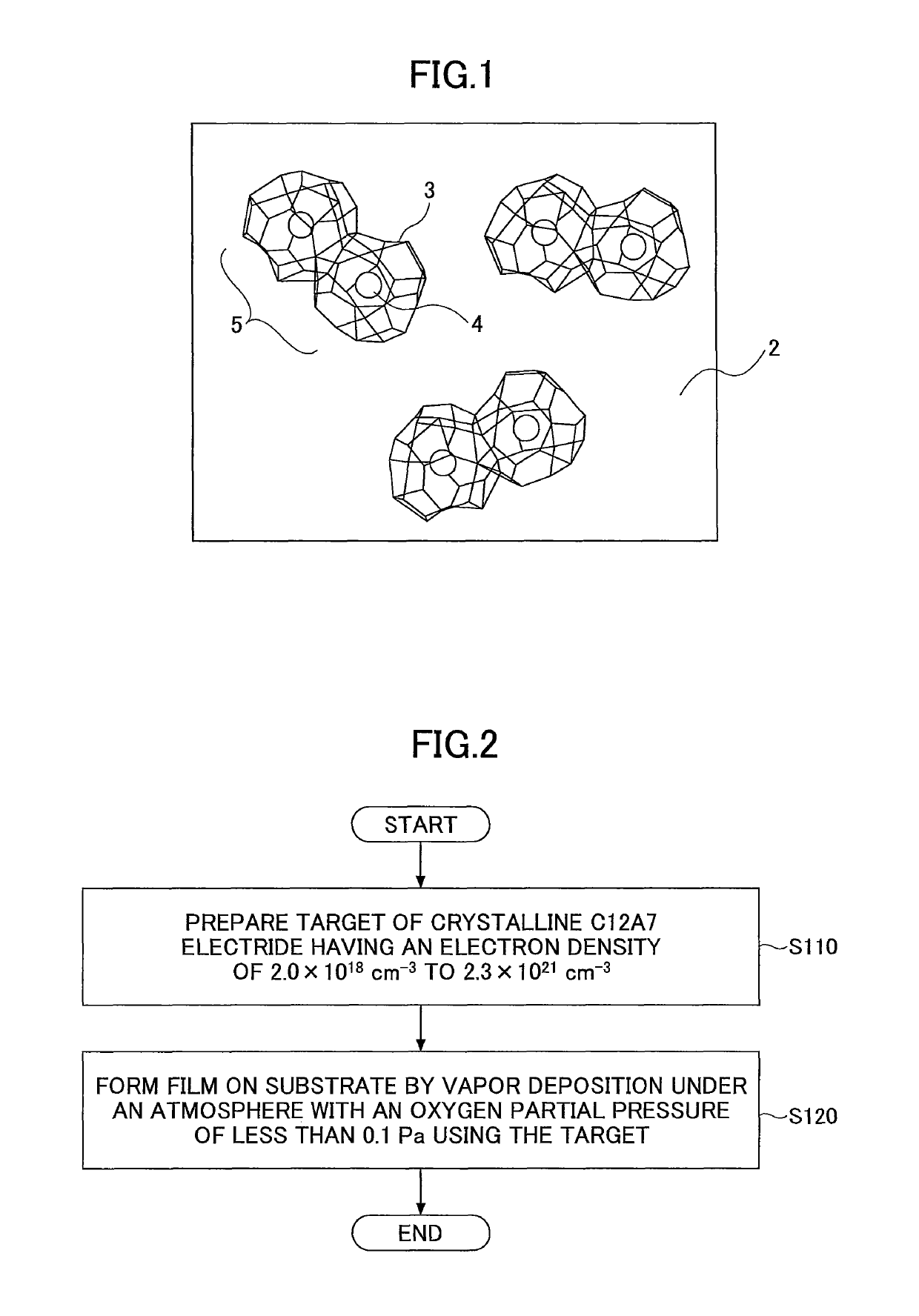
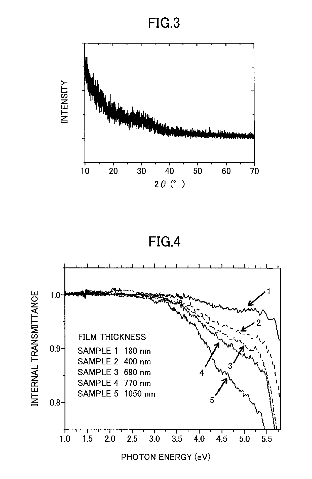
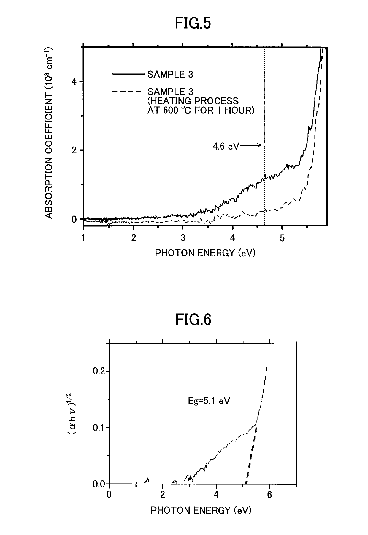

Image

  • C12A7 electride thin film fabrication method and C12A7 electride thin film
  • C12A7 electride thin film fabrication method and C12A7 electride thin film
  • C12A7 electride thin film fabrication method and C12A7 electride thin film

Examples


example 1

Target Fabrication

[0133]First, a raw material powder was obtained by preparing and mixing CaO powder and Al2O3 powder to a molar ratio of 12:7. The raw material powder was heated to 1350° C. in air to fabricate a bulk of crystalline C12A7.

[0134]Then, the crystalline C12A7 bulk was pulverized into powder, and the powder was press-molded through cold isostatic pressing to obtain a crystalline C12A7 molded body. Further, the molded body was placed in a carbon crucible together with metal aluminum and heated to in a vacuum furnace. In the carbon crucible, the molded body and the metal aluminum were separately held. The temperature was heated to 1300° C. and held for 6 hours, and in this way, a crystalline C12A7 electride sintered body was obtained.

[0135]The sintered body was then cut into a disk shape with a thickness of 5 nm and a diameter of 3 inches, and the disk-shaped sintered body was fixed to a Cu backing plate using In to obtain a sputtering target (simply referred to as “target...

example 2

[0167]Sample 6 was fabricated by forming an amorphous C12A7 electride thin film on a substrate in the same manner as the above Example 1. However, in Example 2, the pre-sputtering process using He gas was not conducted. Instead, before using the crystalline C12A7 electride target, the surface of the crystalline C12A7 electride target was polished with a diamond file. Note that the sputtering process using Ar gas was conducted for 2 hours in the present example. Other processing conditions were the same as those used for fabricating Sample 1 of Example 1.

[0168]FIG. 7 illustrates internal transmittance measurement results of Sample 6. Note that in FIG. 7, the internal transmittance measurement results of Sample 2 is indicated along with the internal transmittance measurement results of Sample 6.

[0169]As can be appreciated from FIG. 7, a substantial decrease in transmittance could be observed in Sample 6 at the position of the photon energy of 4.6 eV.

[0170]Thus, it could be confirmed t...

example 3

[0171](Work Function of Amorphous C12A7 Electride Thin Film)

[0172]A sample (Sample 7) having an amorphous C12A7 electride thin film with a thickness of 10 nm formed on an ITO was fabricated by performing the sputtering process for 4 minutes using a glass substrate with ITO (indium tin oxide) instead of a silica glass substrate. Note that other than the above processing conditions, Sample 7 was fabricated in the same manner as Example 1.

[0173]The work function of Sample 7 was measured by ultraviolet photoelectron spectroscopy. In order to obtain a clean surface, measurement was performed under ultra-high vacuum (10−7 Pa), and organic matter was removed from the surface by Ar sputtering before measurement. Also, X-ray photoelectron spectroscopy was performed before and after the Ar sputtering process to confirm that the thin film sample has not been damaged. Further, a DC voltage (bias voltage) was applied to Sample 7 so that Sample 7 may be at a negative potential with respect to the...


PUM

PropertyMeasurementUnit
electron densityaaaaaaaaaa
partial pressureaaaaaaaaaa

Abstract

A C12A7 electride thin film fabrication method includes a step of forming an amorphous C12A7 electride thin film on a substrate by vapor deposition under an atmosphere with an oxygen partial pressure of less than 0.1 Pa using a target made of a crystalline C12A7 electride having an electron density within a range of 2.0×1018 cm−3 to 2.3×1021 cm−3.

Description

CROSS-REFERENCE TO RELATED APPLICATION[0001]The present application is a continuation application filed under 35 U.S.C. 111(a) claiming benefit under 35 U.S.C. 120 and 365(c) of PCT International Application No. PCT / JP2013 / 066850 filed on Jun. 19, 2013 and designating the U.S., which claims priority to Japanese Patent Application No. 2012-139197 filed on Jun. 20, 2012, Japanese Patent Application No. 2012-151848 filed on Jul. 5, 2012, Japanese Patent Application No. 2013-037851 filed on Feb. 27, 2013, Japanese Patent Application No. 2013-071154 filed on Mar. 29, 2013, and Japanese Patent Application No. 2013-071163 filed on Mar. 29, 2013. The entire contents of the foregoing applications are incorporated herein by reference.BACKGROUND OF THE INVENTION[0002]1. Field of the Invention[0003]The present invention relates to a C12A7 electride thin film fabrication method and a C12A7 electride thin film.[0004]2. Description of the Related Art[0005]Crystalline C12A7 has a representative com...

Claims


Application Information

Patent Timeline
Patent Type & Authority Patents(United States)
IPC IPC(8): C23C14/34H01B1/08C23C14/08C23C14/35C04B35/44C04B35/626H01L51/52
CPCH01B1/08C04B35/44C04B35/62645C23C14/08C23C14/3414C23C14/35C23C14/082H01L51/5221C04B2235/3208C04B2235/664H10K50/82
Inventor HOSONO, HIDEOTODA, YOSHITAKEHAYASHI, KATSUROITO, SETSUROWATANABE, SATORUMIYAKAWA, NAOMICHIWATANABE, TOSHINARIITO, KAZUHIRO
Owner AGC INC
Learn More