
Microstructural architecture to enable strain relieved non-linear complex oxide thin films

a thin film, non-linear technology, applied in the direction of capacitors, semiconductor devices, semiconductor/solid-state device details, etc., can solve the problems of film strain, increase lattice parameter and unit cell volume, and introduce film strain, so as to reduce thermal strain, reduce lattice parameter and unit cell volume, and reduce lattice volume

Active Publication Date: 2018-07-24
ARMY US SEC THE
View PDF33 Cites 1 Cited by
  • Summary
  • Abstract
  • Description
  • Claims
  • Application Information

AI Technical Summary

Benefits of technology

This patent provides a method for making a high-quality thin film that can be used in RF and MW tunable devices. The film has a unique microstructural architecture that allows it to relax and adapt to changes in its surrounding environment. This design helps to mitigate the degradation of the film's performance caused by thermal strain. The method is applicable to different substrates and can help to improve the performance of integrated devices. Ultimately, this invention provides a cost-effective and scalable solution for making high-quality thin films that can be used in various applications.

Problems solved by technology

Effect of film defects: Oxygen vacancies are an inherent defect in both epitaxial and non-epitaxial NLCO films and these defects also introduce strain (bulk strain) into the film.
Specifically, oxygen vacancies affect nearest neighbor distance by reducing the Coulomb attractive force between cation and anions in the ionic lattice, resulting in an increased lattice parameter and unit cell volume, hence introduces film strain.
Furthermore, non-linear thermodynamic models have shown that such tensile strain results in a minimum of 20% deterioration in the relative dielectric permittivity of SrTiO3 thin films on Si substrates with respect to its bulk counterpart.
Therefore even though the structural defects are significantly reduced and crystalline grains are grown large in the film during the past-annealing process the films' cannot have desirable dielectric properties exhibiting both high dielectric Q and high dielectric constant / tuning because of thermal strain in the film.
Thus, the CTE mismatch between the film and the substrate which determines the thermal strains becomes a significant parameter that impacts the films dielectric response.
Lower annealing temperatures, which impart incomplete film crystallinity, serves to improve dielectric Q, however the lower processing temperatures are not effective in elevating the dielectric constant of the film, and as such, the films possess low permittivity / minimal tunability, hence the ability to promote device miniaturization is diminished since the size of the tunable device (resonator, filter, phase shifter etc.) depends on the inverse of the square root of the dielectric constant of the NLCO whereby the larger the dielectric constant the smaller the device component.
Additionally, lower annealing / processing temperatures lead to smaller grain sizes, which in its lowest limit results in a large grain boundary area (enhanced leakage path) causing high leakage currents resulting in excessive power draw and often causes premature voltage breakdown of the film.
The major drawbacks of such substrates are their high cost and small-size-geometry availability ($50-$500+ for ˜1×1-in2·pieces) and they are non-standard to semiconductor foundry processing industry.
Aside from the direct substrate cost and the limited size availability, the inherent brittleness of ceramic substrates, which manifests into wafer-dicing issues via device singulation (i.e., device breakage), thereby lowering the device yield per substrate, further compromises the device / materials affordability criteria.
Unfortunately achieving such a thick buffer layer film is difficult due to the fact that most films have a critical thickness after which they become relaxed, hence laden with defects and / or micro-cracks which degrades performance.
Additionally, growth of such thick buffer layers is not practical from the prospective of extended growth times (e.g., for sputter deposition on the order of several hours are required to deposit several hundred nanometers of NLCO films, hence significantly longer process times are necessary to deposit microns of film) with its associated elevated cost.
Although fairly successful for simultaneously achieving reasonable Q and high permittivity / wide-tunability, the premise that films were grown on an MgO substrate, which is a non-device relevant substrate material, causes it to be non-compliant with the device affordability and manufacturability requisites.
Finally, this strain mitigation strategy puts forward added processing complexity in that it requires a two-step growth process (buffer layer film+active NLCO film) and this added complexity is undesirable from the foundry processing point-of-view.
Although this is a successful approach to enable strain relieved SrTiO3 films on device relevant PtSi substrates this method is only useful for solution derived / synthesized thin films, hence this method is fabrication method-limited.
Additionally this approach required long post-deposition annealing times (˜2 hrs. at 750° C.) to impart crystallinity to the film, such extended annealing schedules translate to longer foundry times which result in higher manufacturing costs, hence violate the device affordability criteria.
From the prior art summarized herein the mitigation of film strain to achieve a high permittivity and low dielectric loss (high dielectric Q) NLCO films in concert with other performance, manufacturing and affordability criteria is not easily achieved.

Method used


Image

  • Microstructural architecture to enable strain relieved non-linear complex oxide thin films
  • Microstructural architecture to enable strain relieved non-linear complex oxide thin films
  • Microstructural architecture to enable strain relieved non-linear complex oxide thin films

Examples


Embodiment Construction

[0038]The present invention will now be described more fully with reference to the accompanying drawings, in which exemplary embodiments of the invention are shown. In the drawings, the thicknesses of layers and regions are exaggerated for clarity.

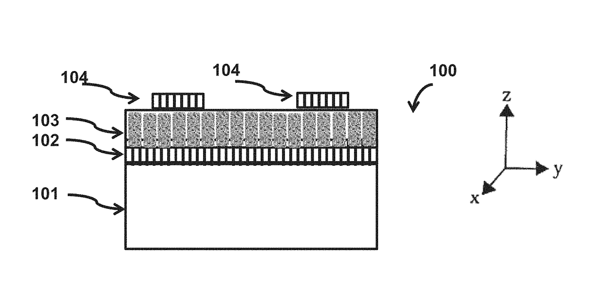
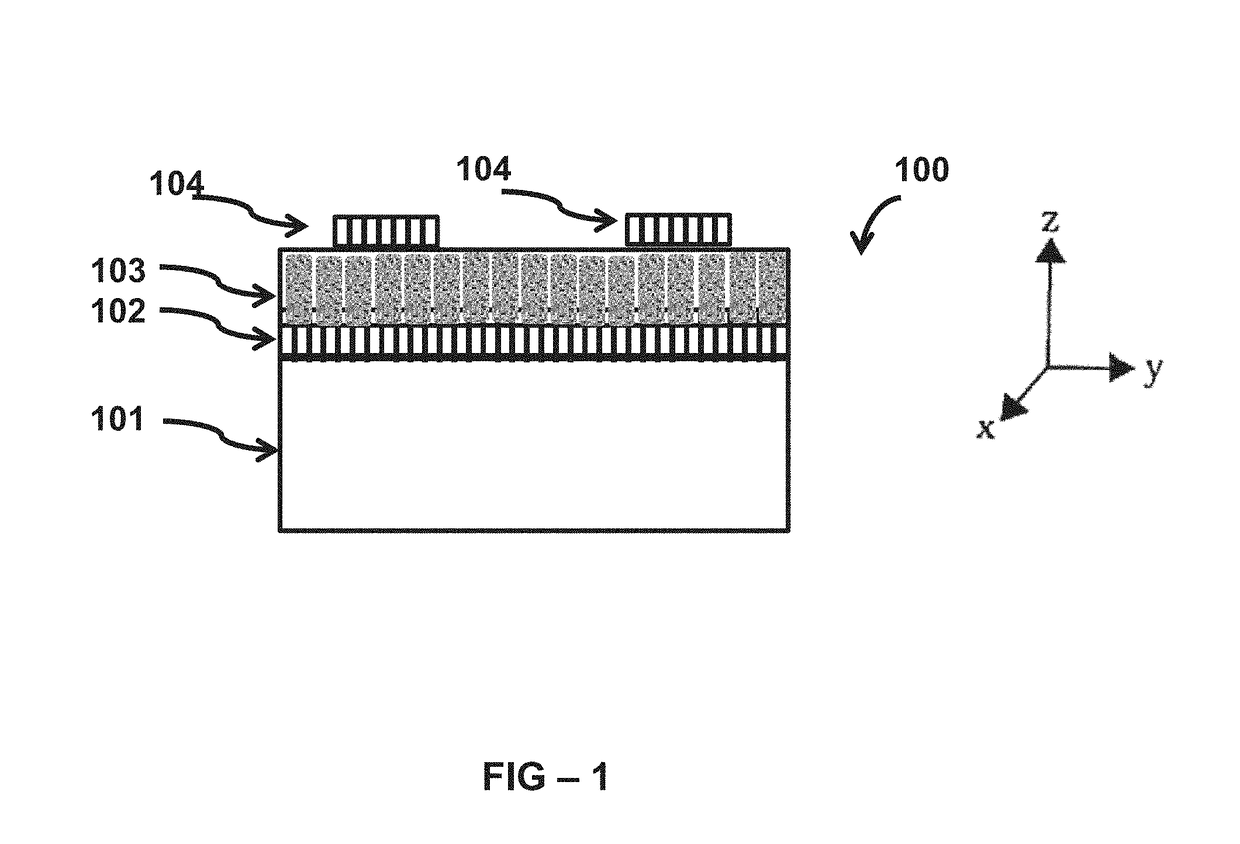
[0039]An integrated NLCO thin film heterostructure with a tailored microstructure architecture design and a method of fabrication thereof, inclusive, is provided. The tailored microstructure architecture design mitigates the undesirable effects of thermal strain, hence provides strain relief, which enables the desirable simultaneous achievement of a high permittivity and high dielectric Q / low dielectric loss in concert with one another. The high dielectric permittivity promotes device miniaturization and wide tunability, while the low loss serves to minimize signal attenuation, reduce device operational power and increases operational range. The material design and fabrication method thereof; enables enhanced performance, low cost NLCO-bas...


PUM

PropertyMeasurementUnit
temperatureaaaaaaaaaa

Abstract

An integrated non-linear complex oxide thin film heterostructure with a tailored microstructure architecture design and a method of fabrication thereof, inclusive, is provided. The tailored microstructure architecture design mitigates the undesirable effects of thermal strain, hence provides strain relief, which enables the desirable simultaneously achievement of a high permittivity and high dielectric Q / low dielectric loss in concert with one another. The material design and fabrication method thereof; enables enhanced performance, low cost NLCO-based tunable devices which possess desirable attributes including, but are not limited to, tunable device miniaturization, wide tunability, minimization of signal attenuation, reduced device operational power and enhanced operational range. Furthermore, the materials and related process science protocols are complementary metal oxide semiconductor compatible, scalable and affordable.

Description

CROSS-REFERENCE TO RELATED APPLICATIONS[0001]This application claims the benefit of U.S. Provisional Patent Application No. 62 / 211,076 filed on Aug. 28, 2015 by inventors Melanie Will-Cole and Daniel Shreiber titled “Microstructural Architecture to Enable Strain Relieved Non-Linear Complex Oxide Thin Films” which is hereby incorporated herein by reference in its entirety including all attachments, appendices and figures filed with U.S. Non-Provisional Patent Application No. 62 / 211,076 filed on Aug. 28, 2015. This application is also a continuation-in-part of U.S. Non-Provisional patent application Ser. No. 14 / 488,771 filed on Sep. 17, 2014 by inventor Melanie Will-Cole titled “Integrated Composite Perovskite Oxide Heterostructure” which is also hereby incorporated herein by reference in its entiretyGOVERNMENT INTEREST[0002]The invention described herein may be manufactured and used by or for the Government of the United States of America for government purposes without the payment o...

Claims


Application Information

Patent Timeline
Patent Type & Authority Patents(United States)
IPC IPC(8): H01L49/02H01L23/66H10N97/00
CPCH01L28/55H01L28/65H01L23/66H01L2223/6683
Inventor SHREIBER, DANIELWILL-COLE, MELANIE
Owner ARMY US SEC THE
Learn More