


Quick Research
Generate reliable direction feasibility study reports for your R&D in just a few steps.

Technical Q&A
Discover and master advanced knowledge NOW. Basics, ideas, possibilities, all at once.

Find Solutions
As an expert in R&D theories, this can generate solutions to your technical problems instantly.

Evaluate Feasibility
Analyze your overall solution with one click, know your potential R&D risks in advance.

Monitor Landscape
Get weekly tech updates, stay abreast of the latest tech innovations and key insights.
Single electron memory having carbon nano tube structure and process for making it
A carbon nanotube and memory technology, applied in nanostructure manufacturing, nanotechnology for information processing, nanotechnology for materials and surface science, etc., can solve the problem of low device integration, limit integration, and affect device stability. to avoid the doping process and reduce the preparation steps
- Summary
- Abstract
- Description
- Claims
- Application Information
AI Technical Summary
Problems solved by technology
Method used
Image


Examples
Embodiment 1
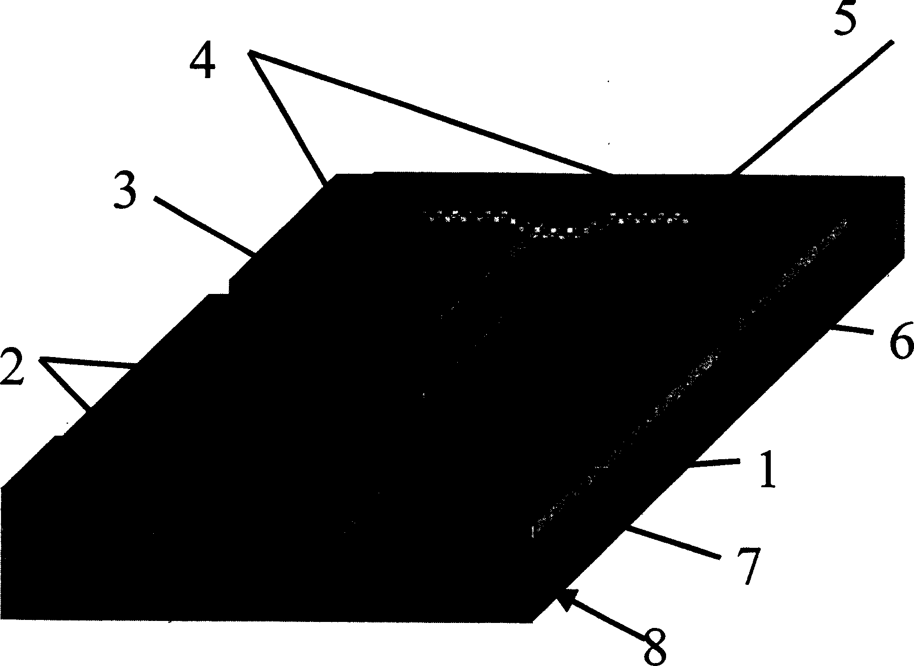
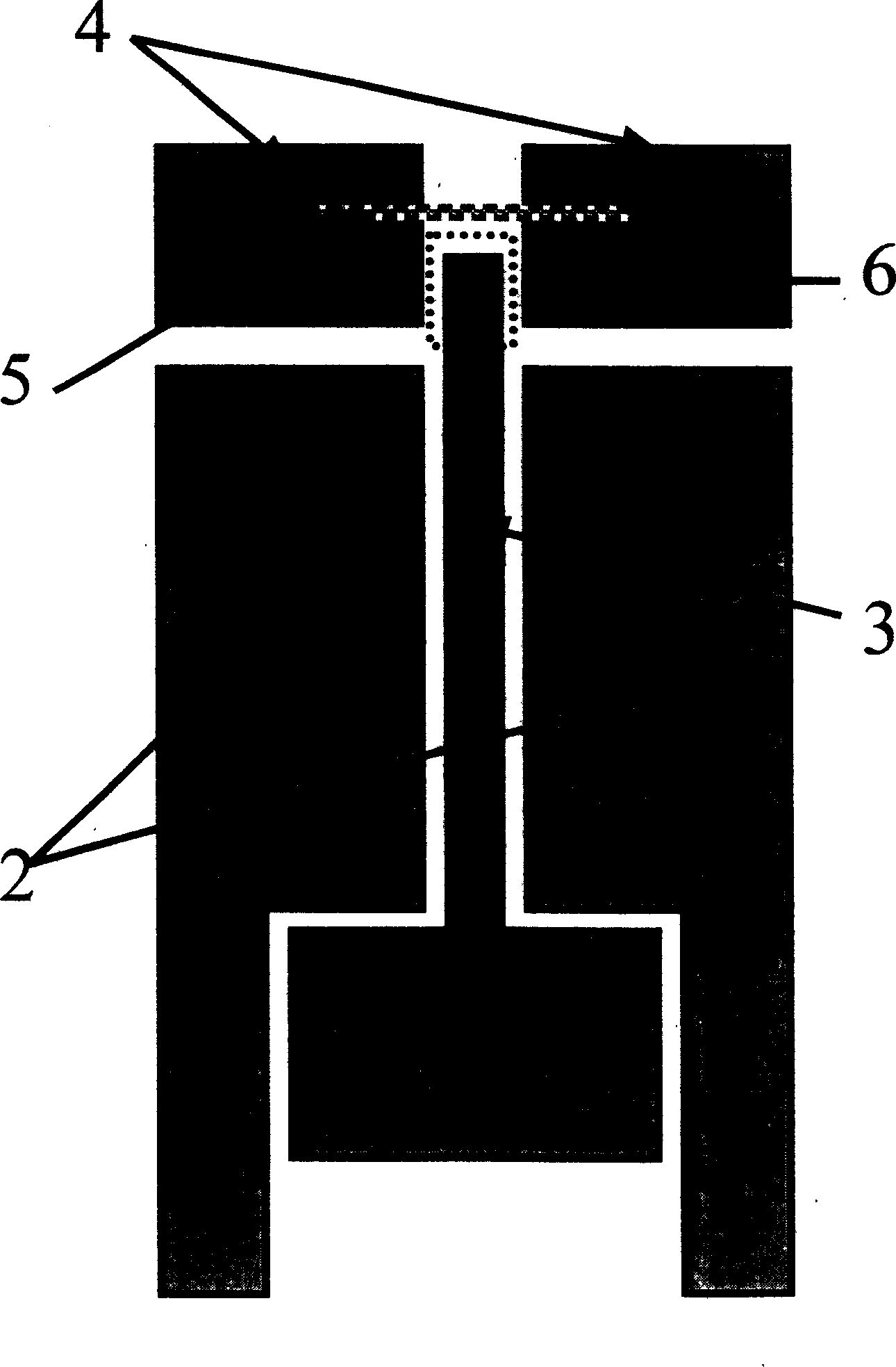
[0038] according to figure 1 A single-electron memory having a carbon nanotube structure of the present invention was fabricated.
[0039] Choose (001) oriented silicon as substrate 8, use dry oxygen oxidation method, oxidation temperature is 900°C, oxidize a silicon dioxide insulating layer 7 with a thickness of 25 nanometers, and prepare a silicon dioxide insulating layer 7 by molecular beam epitaxy (MBE). A polysilicon layer with a thickness of 20 nanometers is heavily doped with arsenic to become an n-type semiconductor layer with a doping concentration of 5×10 13 -2 .
[0040] In the prepared silicon layer, the electrode area 4, the data line pin 1, the control grid 2 of the nanowire and the nanowire 3 are prepared by using the electron beam photolithography method and the dry etching technology. The pin width of the data line is 80 nanometers; the size of the control gate of each nanowire is 80 nanometers wide and 80 nanometers long; the length of the nanowire is 120 n...
Embodiment 2
[0043] according to figure 1 A single-electron memory having a carbon nanotube structure of the present invention was fabricated.
[0044] (001)-oriented silicon is selected as the substrate 8, and a silicon dioxide insulating layer 7 with a thickness of 25 nanometers is oxidized by using a dry oxygen oxidation method at an oxidation temperature of 900°C. A gold layer with a thickness of 30 nm was prepared by electron beam evaporation.
[0045] In the prepared gold layer, the electrode area 4, the data line pin 1, the control gate 2 of the nanowire and the nanowire 3 are prepared by electron beam photolithography and etching technology. The pin width of the data line is 90 nanometers; the size of the control gate of each nanowire is 100 nanometers wide and 100 nanometers long; the length of the nanowire is 160 nanometers long and 40 nanometers wide; wide; gold electrode 4, including two 30 nanometers thick, 50 nanometers wide, 50 nanometers long electrodes of carbon nanotube...
Embodiment 3
[0048] according to Figure 8 A single-electron memory having a carbon nanotube structure of the present invention was fabricated.
[0049] Choose (001) oriented silicon as substrate 8, use dry oxygen oxidation method, oxidation temperature is 900°C, oxidize a silicon dioxide insulating layer 7 with a thickness of 25 nanometers, and prepare a silicon dioxide insulating layer 7 by molecular beam epitaxy (MBE). A polysilicon layer with a thickness of 20 nanometers is heavily doped with arsenic to become an n-type semiconductor layer with a doping concentration of 6×10 13 -2 .
[0050] In the prepared silicon layer, the data wire pin 1 , the control grid 2 of the nanowire and the nanowire 3 are prepared by using an electron beam photolithography method and a dry etching technology. The pin width of the data line is 80 nanometers; the size of the control gate of each nanowire is 80 nanometers wide and 80 nanometers long; the length of the nanowire is 110 nanometers long, 30 nano...
PUM
 Abstract
Description
Claims
Application Information
 - R&D Engineer
- R&D Manager
- IP Professional
- Industry Leading Data Capabilities
- Powerful AI technology
- Patent DNA Extraction
Browse by: Latest US Patents, China's latest patents, Technical Efficacy Thesaurus, Application Domain, Technology Topic, Popular Technical Reports.
© 2024 PatSnap. All rights reserved.Legal|Privacy policy|Modern Slavery Act Transparency Statement|Sitemap|About US| Contact US: help@patsnap.com