Method for manufacturing double-side flexible printed circuit board

一种制造方法、柔性印刷的技术,应用在印刷电路制造、印刷电路、印刷电路等方向,能够解决耐热性不理想、易收缩、贴合部位精度要求很高等问题

Inactive Publication Date: 2005-01-05
SONY GRP CORP
View PDF6 Cites 1 Cited by
  • Summary
  • Abstract
  • Description
  • Claims
  • Application Information

AI Technical Summary

Problems solved by technology

[0003] However, when the double-sided flexible printed circuit board of (i) is used, since the adhesive is thermoplastic, there is a problem that heat resistance is not satisfactory
The double-sided flexible printed circuit board of (ii) has the problem that since the adhesive layer is thermoplastic, the heat resistance is not very good, and it is easy to shrink due to heating, resulting in poor dimensional stability
(iii) The double-sided flexible printed circuit board has the problem that, on the non-thermoplastic polyimide film, it is an electrolytic copper plating layer containing a copper sputtered film, and its peel strength is relatively low, and it is difficult to withstand the heat and humidity under the condition of heating and humidification. Unsatisfactory long-term aging characteristics and poor reliability
[0005] However, when the polyamic acid layers are bonded to each other under high pressure and high temperature conditions after patterning the metal foil, there is a concern that moisture generated during imidization may not escape from the polyimide layer. emitted, which corrodes the metal foil
At the same time, there are also problems that in order to form patterns on both sides, the processability and manufacturing efficiency are reduced, and the precision of the bonding part is required to be high.

Method used


Image

  • Method for manufacturing double-side flexible printed circuit board
  • Method for manufacturing double-side flexible printed circuit board
  • Method for manufacturing double-side flexible printed circuit board

Examples


Embodiment 1

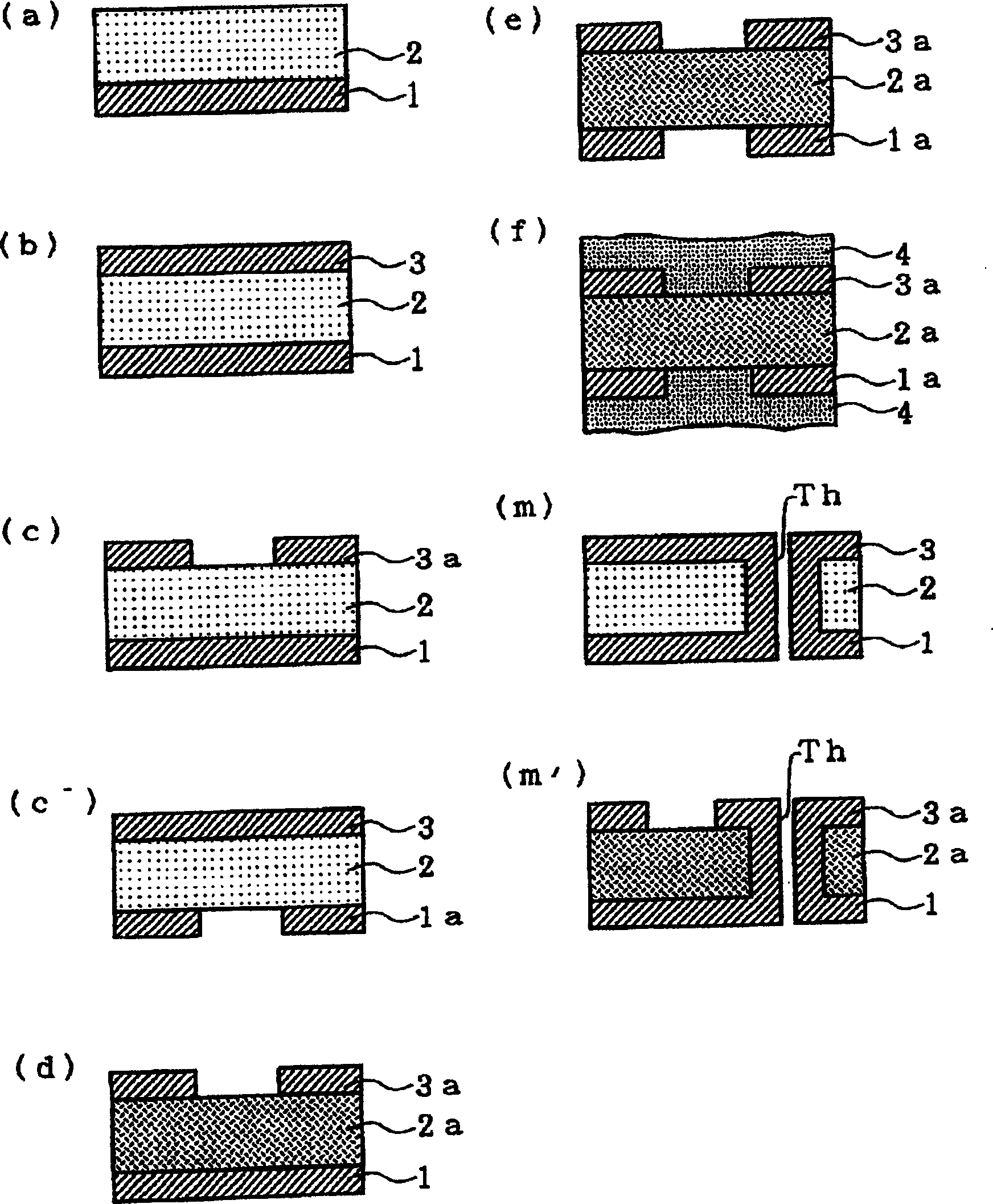
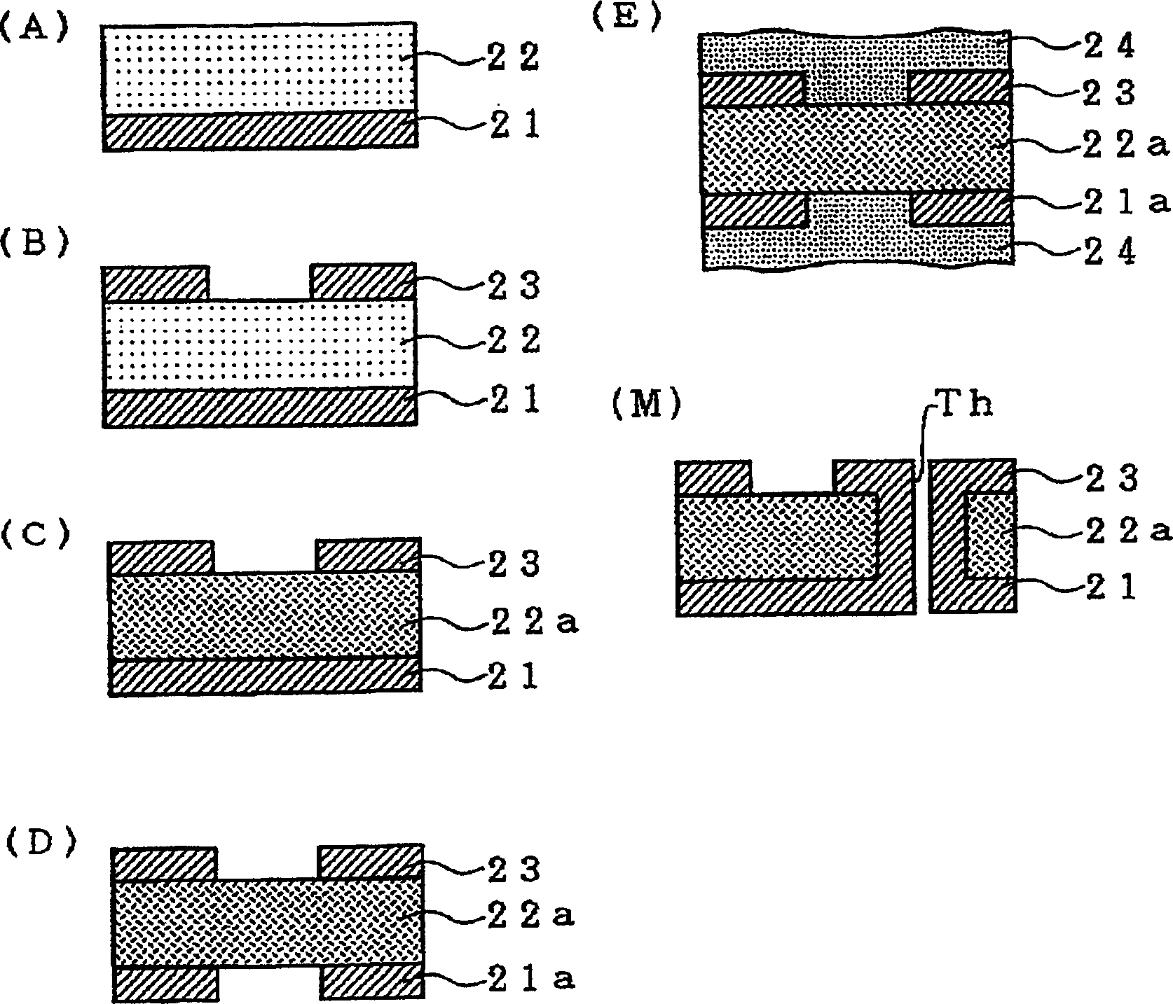
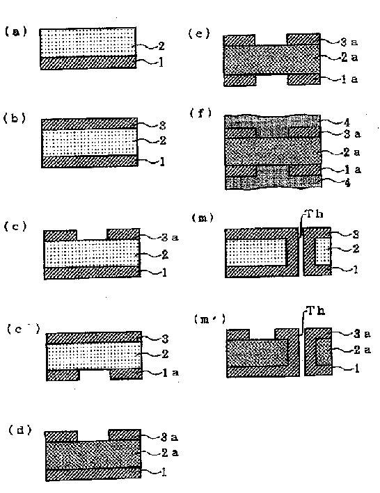
[0073] The polyamic acid varnish obtained in the reference example was coated on the lower layer copper foil with a thickness of 12 μm, and the solvent was evaporated and removed in a continuous furnace at 80 to 170° C. to form a polyamic acid layer as a polyimide precursor layer.

[0074] Next, overlap the upper layer copper foil with a thickness of 12 μm on the polyamic acid layer, and use a 140°C vacuum hot press (surface pressure 70Kg / cm 2 ) for thermocompression bonding.

[0075] Next, after covering the surface of the lower layer copper foil with a protective film, a protective layer for the conductor circuit pattern is formed on the upper layer copper foil, and the upper layer copper foil is etched with an etching solution such as copper chloride aqueous solution to form an upper layer circuit layer. Subsequently, the protective layer and the protective film of the conductive circuit pattern are peeled off.

[0076] Next, put the laminate formed by the lower copper foi...

Embodiment 2

[0089] The polyamic acid varnish obtained in the reference example was coated on a 12 μm thick lower layer copper foil, and the solvent was evaporated in a continuous furnace at 80 to 170° C. to form a polyamic acid layer as a polyimide precursor layer.

[0090] Next, an upper wiring layer is formed on the polyamic acid layer by using a semi-additive method. That is, after the protective film is pasted on the surface of the lower copper foil, a 200 Å thick Ni layer is deposited on the polyamic acid layer by sputtering, and a 1000 Å thick Cu layer is deposited on this layer. A protective layer of conductive circuit patterns is formed on the film. Then use the electrolytic plating method to deposit an electrolytic copper plating layer with a thickness of 18 μm, and then peel off the protective layer of the conductive circuit pattern. The entire surface is subjected to soft etching with a mixed solution of hydrogen peroxide and sulfuric acid, whereby the upper wiring layer 23 is...

Embodiment 3

[0103] The polyamic acid varnish obtained in the reference example was coated on a 12 μm thick lower layer copper foil, and the solvent was evaporated in a continuous furnace at 80 to 170° C. as a polyimide precursor layer to form a polyamic acid layer.

[0104] Next, superimpose a 12 μm thick upper layer copper foil on the polyamic acid layer, and use a 200°C extrusion roll (surface pressure 60kg / cm 2 ) for hot pressing.

[0105] For the obtained laminated body consisting of lower layer copper foil / polyamic acid layer / upper layer copper foil, through-holes for through-holes are processed with an NC drill, and a copper layer is formed on the inner wall of the through-holes by a conventional method to obtain through-holes. , to ensure conduction between the upper copper foil and the lower copper foil.

[0106] Next, after covering the surface of the lower layer copper foil with a protective film, a protective layer of a conductor circuit pattern is formed on the upper layer co...


PUM


Abstract

A double-sided flexible printed board is manufactured by the following steps of: (a) forming a polyimide precursor layer 2 on a first metal layer 1; (b) forming a second metal layer 3 on the polyimide precursor layer 2; (c) patterning the second metal layer 3 to form a second circuit layer 3a or (c') patterning the first metal layer 1 to form a first circuit layer 1a; and (d) imidating the polyimide precursor layer 2 to form a polyimide insulating layer 2a.

Description

technical field [0001] The present invention relates to a method for manufacturing a double-sided flexible printed circuit board using a polyimide-based insulating layer. Background technique [0002] As the previous polyimide-based double-sided flexible printed circuit boards, generally used are (i) made of copper foil / thermoplastic polyimide adhesive / non-thermoplastic polyimide Substrate composed of imide film / thermoplastic polyimide adhesive / copper foil layer, (ii) substrate composed of copper foil / thermoplastic polyimide adhesive layer / copper foil layer, or using Non-thermoplastic polyimide tape casting film, combined with sputtering method and electrolytic plating method to form a copper layer substrate, (iii) copper foil / non-thermoplastic polyimide film / copper sputtering film and electrolytic copper electroplating film formed substrate. [0003] However, when the double-sided flexible printed wiring board of (i) is used, since the adhesive is thermoplastic, there is ...

Claims


Application Information

Patent Timeline
Patent Type & Authority Patents(China)
IPC IPC(8): H05K3/40H05K1/03H05K3/00H05K3/06H05K3/38
CPCH05K3/38H05K1/0346H05K3/06Y10S428/901H05K3/0011H05K2201/0154H05K2203/1105Y10T29/49126Y10T29/49155Y10T29/49165Y10T428/24917Y10T428/31681Y10T428/31721
Inventor 栗田英之渡边正直
Owner SONY GRP CORP
Why Eureka
Try Eureka