INP wafer thinning and polishing process method

A technology of thinning and polishing, process method, applied in the direction of sustainable manufacturing/processing, climate sustainability, final product manufacturing, etc., can solve the problems that the N-side metal cannot be operated at one time, the back of the wafer is rough, and the processing cost is high. Achieve the effects of improving the warping problem, smoothing the wafer surface, and reducing processing costs

Pending Publication Date: 2022-08-05
FUJIAN Z K LITECORE LTD
View PDF0 Cites 0 Cited by
  • Summary
  • Abstract
  • Description
  • Claims
  • Application Information

AI Technical Summary

Problems solved by technology

However, the existing technology has the following problems: 1) Mechanical damage is caused after thinning, and the back of the wafer is rough; 2) High-speed laser products have a thick passivation layer and poor heat dissipation, and wafers will warp to varying degrees after thinning. 3) High-speed laser products need to be thinned to 80-100um, but it is difficult to meet the requirements simply by thinning, and it is easy to crack; 4) N-side metal cannot be operated at one time, and the processing cost is high

Method used


Image

  • INP wafer thinning and polishing process method
  • INP wafer thinning and polishing process method
  • INP wafer thinning and polishing process method

Examples


Embodiment 1

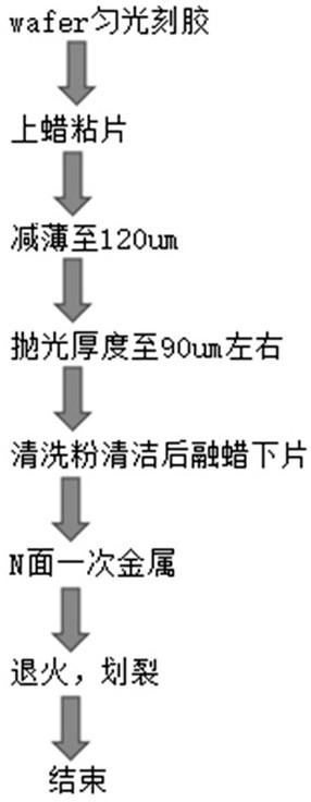
[0038] (1) Wafer the wafer with photoresist, thin it to 120um, and measure the thickness.

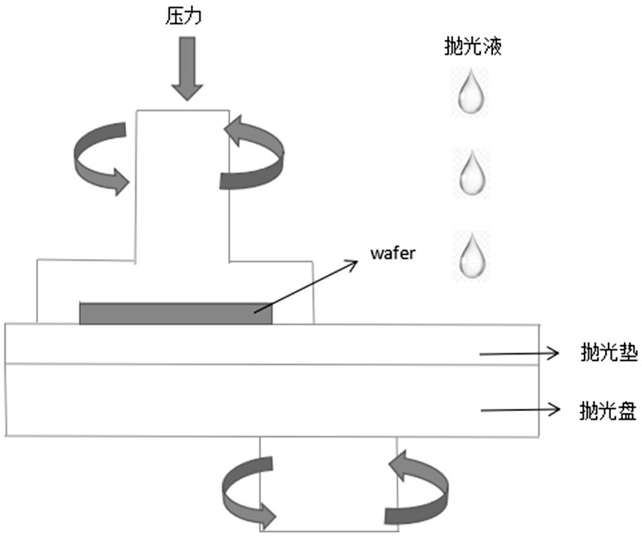
[0039] (2) Remove the wafer from the thinned glass plate, replace it with a polishing plate, and contact the wafer with the polishing pad.

[0040] (3) Polishing for 15 minutes, polishing the wafer to 80-100um, using alumina polishing liquid ASCP2002, the peristaltic pump controls the liquid all the time, the total polishing flow is 250-300ml, the polishing temperature is 25°C, and the polishing pressure is 230g / cm 2 .

[0041] (4) Use absorbent cotton dipped in cleaning powder: water = 100:1 solution for cleaning, then blow dry with nitrogen, and remove the film.

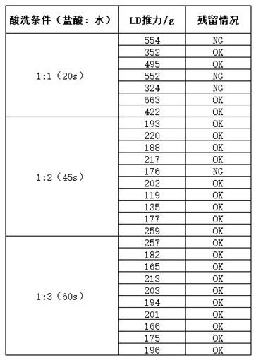
[0042] (5) Wash with hydrochloric acid: water = 1:1 for 20s, and carry out N-side metal coating.

[0043] (6) Annealing, and finally slicing the cleavage strip.

Embodiment 2

[0044] Embodiment 2, embodiment 3 are similar to embodiment 1, and the difference lies in the pickling condition after the next tablet:

[0045] In Example 2, in step (5), use hydrochloric acid: water = 1:2 to clean for 45s, and perform N-face metal coating.

[0046] In Example 3, in step (5), hydrochloric acid: water = 1:3 was used for cleaning for 60s, and N-face metal coating was performed.

[0047] Other steps are the same as in Example 1.


PUM


Abstract

The invention relates to an INP wafer thinning and polishing process method which comprises the following steps: (1) waxing and bonding a wafer with photoresist, and thinning the wafer to 120-125 microns on thinning equipment; (2) the wafer is taken down from the thinning device and placed on a polishing device, and the wafer makes contact with a polishing pad on a polishing disc; (3) polishing is conducted for 10 min to 20 min, and the wafer is polished to 80 micrometers to 100 micrometers; the polishing solution is controlled to be discharged continuously in the polishing process, the polishing temperature is 23-27 DEG C, and the polishing pressure is 180-300 g / cm < 2 >; (4) cleaning and blow-drying the wafer, and then melting wax and discharging the wafer; (5) carrying out primary metal coating on the N surface; and (6) annealing, and then scribing cracking strips. The method is favorable for improving the product performance and obtaining a high-quality chip.

Description

technical field [0001] The invention belongs to the technical field of semiconductor manufacturing, and in particular relates to an INP sheet thinning and polishing process method. Background technique [0002] When the INP wafer is processed to the thinning process, the backside substrate is ground to remove a certain thickness of material, which effectively reduces the volume of the chip package and meets the requirements of heat dissipation and size. After thinning, the thickness is required to be between 100~120um, and the film is unloaded, and then the N-side primary metal coating, the N-side alloy, and the N-side secondary metal coating are respectively performed. However, the existing technology has the following problems: 1) Mechanical damage is caused after thinning, and the back of the wafer is rough; 2) For high-speed laser products, the passivation layer is thick and the heat dissipation is poor. It cannot be improved after alloying; 3) High-speed laser products...

Claims


Application Information

Patent Timeline
Patent Type & Authority Applications(China)
IPC IPC(8): H01L21/02B24B1/00
CPCH01L21/02013B24B1/00Y02P70/50
Inventor 黄惠莺薛正群
Owner FUJIAN Z K LITECORE LTD
Why Eureka
Try Eureka