Reworking method for poor back surface of lithium niobate single-sided polished wafer
A single-side polishing and lithium niobate technology, which is applied in the direction of sustainable manufacturing/processing, climate sustainability, piezoelectric/electrostrictive/magnetostrictive devices, etc., can solve the bad rework of lithium niobate single-side polished sheets method, lithium niobate single-sided polishing sheet scratches, thin thickness, etc., to achieve the effect of improving rework yield, less rework removal, and high flatness
- Summary
- Abstract
- Description
- Claims
- Application Information
AI Technical Summary
Problems solved by technology
Method used
Image
Examples
Embodiment 1
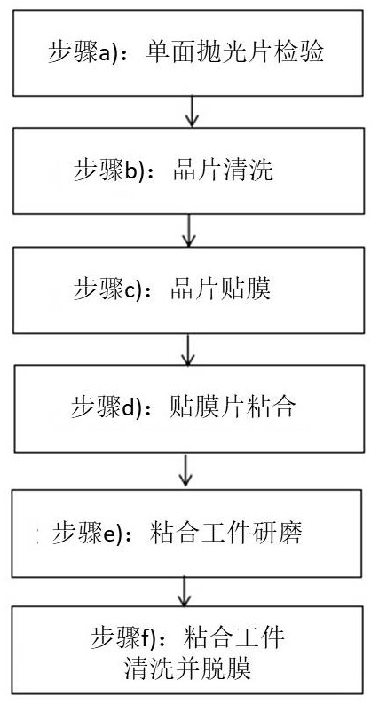
[0038] a) Test the single-sided polished lithium niobate sheet under a yellow strong light with a brightness of 1000 Lux, and measure the thickness of the wafer with defective backside to obtain a defective backside sheet of lithium tantalate with the same thickness;
[0039] b) Put the wafers whose backside defects are detected into alkaline cleaning solutions with concentrations of 10%, 5%, and 3.3% in turn, and carry out ultrasonic cleaning at ultrasonic powers of 28 kHz, 40 kHz, and 200 kHz in turn, and the cleaning temperature is 35 ° C. The cleaning time is 40 minutes in total, which reduces the particle contamination on the surface of the wafer and reduces the rate of subsequent processing splits;
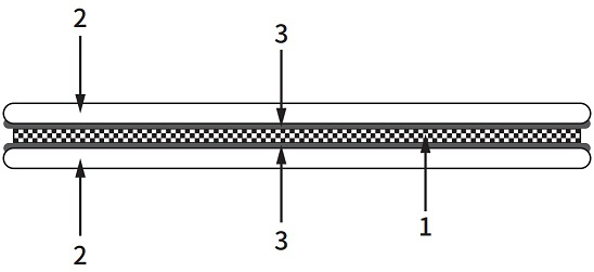
[0040] c) Put the cleaned wafer into the laminating machine, use a 80μm PET composite film, the film tension is -100Mpa, the blade cutting temperature is 70°C, and the blade cuts the film along the reference edge of the wafer at a cutting speed of 2000pps, respectively. Cut ...
Embodiment 2
[0045] a) with embodiment 1;
[0046] b) with embodiment 1;
[0047] c) Put the cleaned wafer into the laminating machine, use a PET composite film with a thickness of 125μm, the film tension is -100Mpa, the blade cutting temperature is 70°C, and the blade cuts the film along the reference edge of the wafer at a cutting speed of 2000pps, respectively. Cut along the arc position of the wafer at a speed of 3500pps to obtain a wafer with a polished surface;
[0048] d) with embodiment 1;
[0049] e) with embodiment 1;
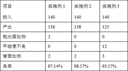
[0050] f) Same as Example 1, obtain reworked lithium niobate single-sided polishing sheet, diameter 100.00mm, thickness 241.8μm, backside roughness 0.18μm, flatness 1.36μm, input 140 pieces, output 138 pieces, the backside is scratched 2 pieces, yield 98.57%.
Embodiment 3
[0052] a) with embodiment 1;
[0053] b) with embodiment 1;
[0054] c) Put the cleaned wafer into the laminating machine, use a PET composite film with a thickness of 200μm, the film tension is -100Mpa, the blade cutting temperature is 70°C, and the blade cuts the film along the reference edge of the wafer at a cutting speed of 2000pps, respectively. Cut along the arc position of the wafer at a speed of 3500pps to obtain a wafer with a polished surface;
[0055] d) with embodiment 1;
[0056] e) with embodiment 1;
[0057] f) Same as Example 1, obtain reworked lithium niobate single-sided polishing sheet, the diameter is 100.00 mm, the thickness is 242.6 μm, the back surface roughness is 0.18 μm, and the flatness is 2.16 μm, 140 pieces were input, and 131 pieces were output , 12 pieces with poor flatness, 3 pieces with scratches on the back, and the yield rate is 93.57%.
[0058] Comparative Examples 1, 2 and 3, as shown in Table 1, the thinner the PET composite film, the...
PUM
| Property | Measurement | Unit |
|---|---|---|
| thickness | aaaaa | aaaaa |
| density | aaaaa | aaaaa |
| thickness | aaaaa | aaaaa |
Abstract
Description
Claims
Application Information
 - Generate Ideas
- Intellectual Property
- Life Sciences
- Materials
- Tech Scout
- Unparalleled Data Quality
- Higher Quality Content
- 60% Fewer Hallucinations
Browse by: Latest US Patents, China's latest patents, Technical Efficacy Thesaurus, Application Domain, Technology Topic, Popular Technical Reports.
© 2025 PatSnap. All rights reserved.Legal|Privacy policy|Modern Slavery Act Transparency Statement|Sitemap|About US| Contact US: help@patsnap.com


