
High-voltage fast recovery diode FRED manufacturing process

A technology for recovering diodes and manufacturing processes, which is applied in semiconductor/solid-state device manufacturing, semiconductor devices, electrical components, etc. It can solve the problems of unfavorable cost optimization and high cost of epitaxial materials, and achieve material cost reduction, material cost reduction, and production cost reduction Effect

Pending Publication Date: 2022-06-24
厦门中能微电子有限公司
View PDF0 Cites 0 Cited by
  • Summary
  • Abstract
  • Description
  • Claims
  • Application Information

AI Technical Summary

Problems solved by technology

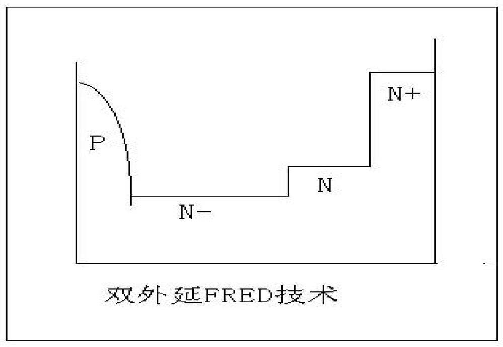
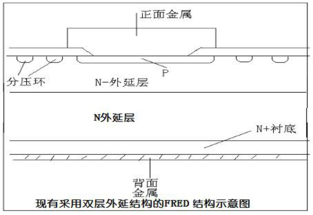
At present, the method of manufacturing FRED with a double epitaxial structure is to grow an epitaxial N- layer on a heavily doped N+ substrate as a substrate for processing. However, in order to improve the reverse recovery performance of FRED and improve the softness of reverse recovery, in fact 1350V The FRED product adopts a double-layer epitaxial structure. The lowermost epitaxial layer adopts an epitaxial layer with a thicker resistivity. The epitaxial thickness is about 30um, and then grows an epitaxial layer with a lighter resistivity. The epitaxial thickness is about 80um. The overall thickness is about 110um. Due to the thicker epitaxial thickness, the cost of epitaxial materials is high, and the cost of epitaxial materials accounts for more than 60% of the processing cost of the entire device. Therefore, the current processing technology is not conducive to cost optimization.

Method used


Image

  • High-voltage fast recovery diode FRED manufacturing process
  • High-voltage fast recovery diode FRED manufacturing process
  • High-voltage fast recovery diode FRED manufacturing process

Examples


Embodiment Construction

[0038] In order to make the objectives, technical solutions and advantages of the present invention clearer, the technical solutions of the present invention will be described clearly and completely below. Obviously, the described embodiments are only some, but not all, embodiments of the present invention. Based on the embodiments of the present invention, all other embodiments obtained by those of ordinary skill in the art without creative work fall within the protection scope of the present invention.

[0039] The test methods or test methods described in the following examples are conventional methods unless otherwise specified; the raw materials and auxiliary agents, unless otherwise specified, are obtained from conventional commercial channels or prepared by conventional methods.

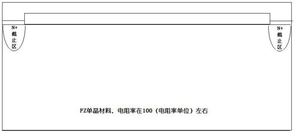
[0040] (1) Form the N+ cut-off ring region. For high-voltage devices above 1200V, a reasonable cut-off ring region is necessary. Phosphorus impurities are implanted, and the implant dose is be...


PUM

PropertyMeasurementUnit
Thicknessaaaaaaaaaa

Abstract

The invention provides a manufacturing process of a high-voltage fast recovery diode (FRED), which comprises the following steps of: (1) forming an N + cut-off ring region, and injecting phosphorus impurities; (2) forming an active region and injecting and annealing an N well of the active region, wherein the injected impurity of the N well is phosphorus impurity; (3) forming a P + voltage dividing ring, injecting boron impurities, and annealing; (4) forming a P well, injecting boron impurities, and annealing; (5) opening a lead hole, enriching P + on the surface of the hole, injecting boron into the P +, and annealing; (6) Pt heavy metal doping and annealing are carried out, and minority carrier lifetime is adjusted; (7) front metal is formed, aluminum-silicon-copper is adopted, and the thickness is about 4 microns; (8) forming a passivation layer; (9) thinning the back surface; (10) carrying out heavy doping injection on the back surface, wherein the injected impurities are phosphorus-based alloy; (11) performing proton injection and annealing on the back surface, wherein the thickness of the whole N-region buffer layer is 10-15 microns; and (12) processing metal on the back surface to obtain the high-voltage fast recovery diode FRED. According to the method, the FRED processing cost can be effectively reduced.

Description

technical field [0001] The invention relates to the technical field of semiconductor components, in particular to a manufacturing process of a high-voltage fast recovery diode FRED. Background technique [0002] Epitaxial Fast Recovery Diode (FRED) is a new type of semiconductor power device prepared by CMOS technology. It is a semiconductor diode with good switching characteristics and short reverse recovery time. It is mainly used in switching power supplies, pulse width modulators, frequency conversion It can be used as a high-frequency rectifier diode, freewheeling diode or damping diode in electronic circuits such as circuit breakers. At present, most FREDs are made of double epitaxial structures. The structure diagram of conventional FREDs is shown in the following figure. figure 1 shown. The double epitaxy FRED technology has two N regions, the most critical of which is the selection of the buffer N region. If the concentration is too low, the expansion of space cha...

Claims


Application Information

Patent Timeline
IPC IPC(8): H01L21/329H01L21/266H01L29/861
CPCH01L29/6609H01L29/861H01L21/266
Inventor 鄢细根黄种德
Owner 厦门中能微电子有限公司
Learn More