Power semiconductor chip packaging structure capable of realizing low-temperature bonding and high-temperature service
A technology for power semiconductors and high-temperature service. It is applied in the direction of semiconductor devices, semiconductor/solid-state device components, and electrical solid-state devices. It can solve problems such as high hardness, unfavorable device reliability, and high brittleness, and achieve good solderability of the coating. The effect of delaying the turbidity of the plating solution and preventing the formation of dendrites
- Summary
- Abstract
- Description
- Claims
- Application Information
AI Technical Summary
Problems solved by technology
Method used
Image
Examples
Embodiment 1
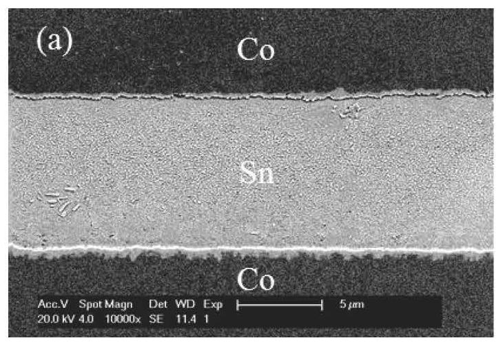
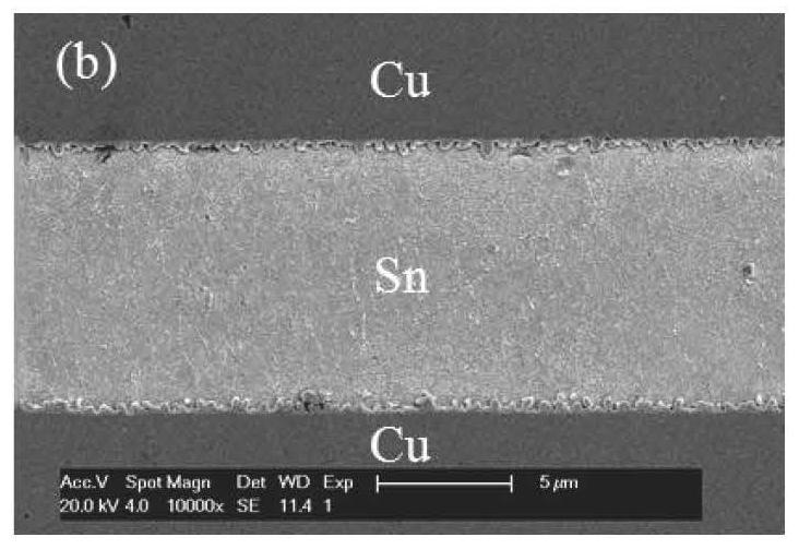
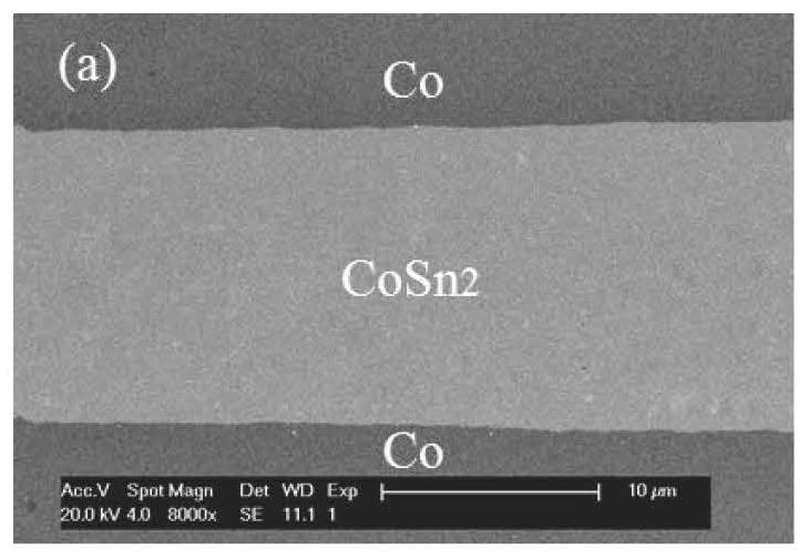
[0032] In the traditional package structure, the gold Ti / Ni / Au layer on the back of the chip and the surface of the Cu layer on the substrate are plated with Co by electroplating. First, the surface of the plated sample was cleaned with dilute sulfuric acid, deionized water and acetone with a concentration of 30 vol%. The low-stress Co electroplating solution was prepared according to the "Electroplating Manual", and the solution composition was: cobalt sulfamate 450g / L, formamide 30mL / L, sodium lauryl sulfate 0.4g / L, saccharin 1.0g / L . Electroplating temperature 40℃, current density 4.0A / dm 2, control the plating time so that the thickness of the Co coating is about 5 μm. The surface of the electroplated Co layer was washed with deionized water and blown dry, and the Sn plating treatment was further performed. Preferably, the components of the electroplating solution are selected to be composed of 20 g / L of stannous sulfate, 90 g / L of sulfuric acid, 3.0 g / L of ferrous sulf...
Embodiment 2
[0034] In the traditional package structure, the gold Ti / Ni / Au layer on the back of the chip and the surface of the Cu layer on the substrate are plated with Co by electroplating. First, the surface of the plated sample was cleaned with dilute sulfuric acid, deionized water and acetone with a concentration of 30 vol%. The low-stress Co electroplating solution was prepared according to the "Electroplating Manual", and the solution composition was: cobalt sulfamate 450g / L, formamide 30mL / L, sodium lauryl sulfate 0.4g / L, saccharin 1.0g / L . Electroplating temperature 40℃, current density 4.0A / dm 2 , control the plating time so that the thickness of the Co coating is about 10 μm. The surface of the electroplated Co layer was washed with deionized water and blown dry, and the Sn plating treatment was further performed. The components of the electroplating solution were selected as 10g / L of stannous sulfate, 100g / L of sulfuric acid, 1.0g / L of ferrous sulfate, 0.5g / L of antimony po...
Embodiment 3
[0036] In the traditional package structure, the gold Ti / Ni / Au layer on the back of the chip and the surface of the Cu layer on the substrate are plated with Co by electroplating. First, the surface of the plated sample was cleaned with dilute sulfuric acid, deionized water and acetone with a concentration of 30 vol%. The low-stress Co electroplating solution was prepared according to the "Electroplating Manual", and the solution composition was: cobalt sulfamate 450g / L, formamide 30mL / L, sodium lauryl sulfate 0.4g / L, saccharin 1.0g / L . Electroplating temperature 40℃, current density 4.0A / dm 2 , control the plating time so that the thickness of the Co coating is about 10 μm. The surface of the electroplated Co layer was washed with deionized water and blown dry, and the Sn plating treatment was further performed. Preferably, the components of the electroplating solution are selected to be composed of 50 g / L of stannous sulfate, 50 g / L of sulfuric acid, 1.0 g / L of ferrous su...
PUM
| Property | Measurement | Unit |
|---|---|---|
| Thickness | aaaaa | aaaaa |
| Thickness | aaaaa | aaaaa |
| Thickness | aaaaa | aaaaa |
Abstract
Description
Claims
Application Information
 - R&D
- Intellectual Property
- Life Sciences
- Materials
- Tech Scout
- Unparalleled Data Quality
- Higher Quality Content
- 60% Fewer Hallucinations
Browse by: Latest US Patents, China's latest patents, Technical Efficacy Thesaurus, Application Domain, Technology Topic, Popular Technical Reports.
© 2025 PatSnap. All rights reserved.Legal|Privacy policy|Modern Slavery Act Transparency Statement|Sitemap|About US| Contact US: help@patsnap.com


