


Quick Research
Generate reliable direction feasibility study reports for your R&D in just a few steps.

Technical Q&A
Discover and master advanced knowledge NOW. Basics, ideas, possibilities, all at once.

Find Solutions
As an expert in R&D theories, this can generate solutions to your technical problems instantly.

Evaluate Feasibility
Analyze your overall solution with one click, know your potential R&D risks in advance.

Monitor Landscape
Get weekly tech updates, stay abreast of the latest tech innovations and key insights.
Preparation method of IGBT (Insulated Gate Bipolar Translator) with self-aligned trench gate structure
A trench gate and self-alignment technology, which is applied in the manufacture of semiconductor/solid-state devices, electrical components, circuits, etc., can solve the problems of unsuitable power semiconductor chips, reduce the requirements of lithography precision, improve the area range, and narrow space The effect of the hole current path
- Summary
- Abstract
- Description
- Claims
- Application Information
AI Technical Summary
Problems solved by technology
Method used
Image


Examples
Embodiment 1
[0056] A method of preparing an IGBT of a self-aligning groove gate structure, including the following steps:
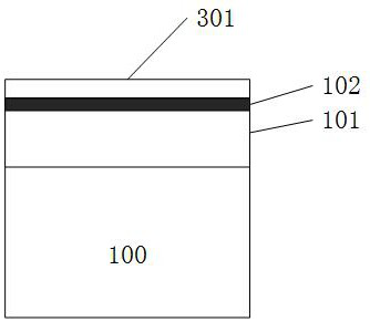
[0057] Step 1: figure 1 As shown, the second conductive type layer A, and the first conductivity type layer are formed by the ion implantation and diffusion process, and then the first hard mask layer is then deposited;
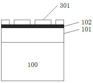
[0058] Step 2: If figure 2 As shown, the first hard mask layer is etched by a photolithography pattern mask;
[0059] Step three: image 3 As shown, the substrate is etched to form a deep trench, and the thermal growth is formed to form a first insulating dielectric layer;
[0060] Step 4: Figure 4 The first conductive layer is deposited;
[0061] Step 5: Figure 5 As shown, the first conductive layer is etched;
[0062] Step 6: Image 6 The third insulating dielectric layer is deposited.
[0063] Step 7: Figure 7 As shown, the etching third insulating dielectric layer is sealed to the first hard mask; the third insulating dielectric layer acts as a mask i...
Embodiment 2
[0073] A method of preparing an IGBT of a self-aligning groove gate structure, including the following steps:
[0074] Step 1: figure 1 As shown, the second conductive type layer A, and the first conductivity type layer are formed by the ion implantation and diffusion process, and then the first hard mask layer is then deposited;
[0075] Step 2: If figure 2 As shown, the first hard mask layer is etched by a photolithography pattern mask;
[0076] Step three: image 3 As shown, the substrate is etched to form a deep trench, and the thermal growth is formed to form a first insulating dielectric layer;
[0077] Step 4: Figure 4 The first conductive layer is deposited;
[0078] Step 5: Figure 5 As shown, the first conductive layer is etched;
[0079] Step 6: Image 6 The third insulating dielectric layer is deposited.
[0080] Step 7: Figure 7 As shown, the etching third insulating dielectric layer is sealed to the first hard mask; the third insulating dielectric layer acts as a mask i...
PUM
| Property | Measurement | Unit |
|---|---|---|
| depth | aaaaa | aaaaa |
| width | aaaaa | aaaaa |
| width | aaaaa | aaaaa |
Abstract
Description
Claims
Application Information
 - R&D Engineer
- R&D Manager
- IP Professional
- Industry Leading Data Capabilities
- Powerful AI technology
- Patent DNA Extraction
Browse by: Latest US Patents, China's latest patents, Technical Efficacy Thesaurus, Application Domain, Technology Topic, Popular Technical Reports.
© 2024 PatSnap. All rights reserved.Legal|Privacy policy|Modern Slavery Act Transparency Statement|Sitemap|About US| Contact US: help@patsnap.com