Alloy/magnetic insulator spin heterojunction and preparation method and application thereof
A heterojunction and insulator technology, which is applied to the parts of electromagnetic equipment, the manufacture/processing of electromagnetic devices, and the selection of materials, can solve the problems of thin film difficulties, high drive magnetization switching current density, etc., and achieve easy flipping and fast switching. Magnetic moment reversal operation, the effect of avoiding power consumption
- Summary
- Abstract
- Description
- Claims
- Application Information
AI Technical Summary
Problems solved by technology
Method used
Image
Examples
preparation example Construction
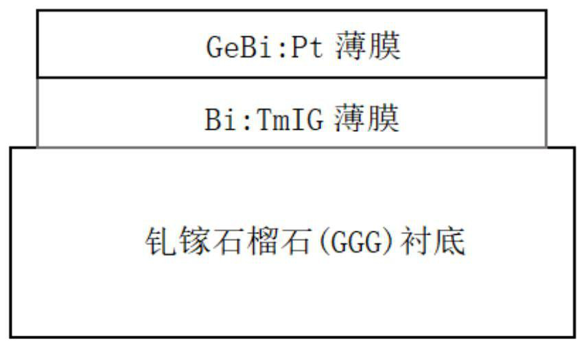
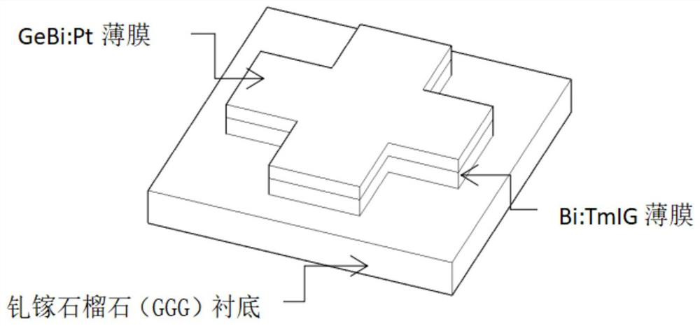
[0034] A method for preparing an alloy / magnetic insulator spin heterojunction device, comprising the following steps:
[0035] Step 1, cleaning the gadolinium gallium garnet substrate;
[0036] Step 2, using liquid phase epitaxy to grow a Bi:TmIG film on the surface of the gadolinium gallium garnet substrate cleaned in step 1;
[0037] Step 3, using the magnetron sputtering method to grow a germanium-bismuth-platinum alloy film on the surface of the Bi:TmIG film obtained in step 2 to obtain the desired alloy / magnetic insulator spin heterojunction.
Embodiment 1
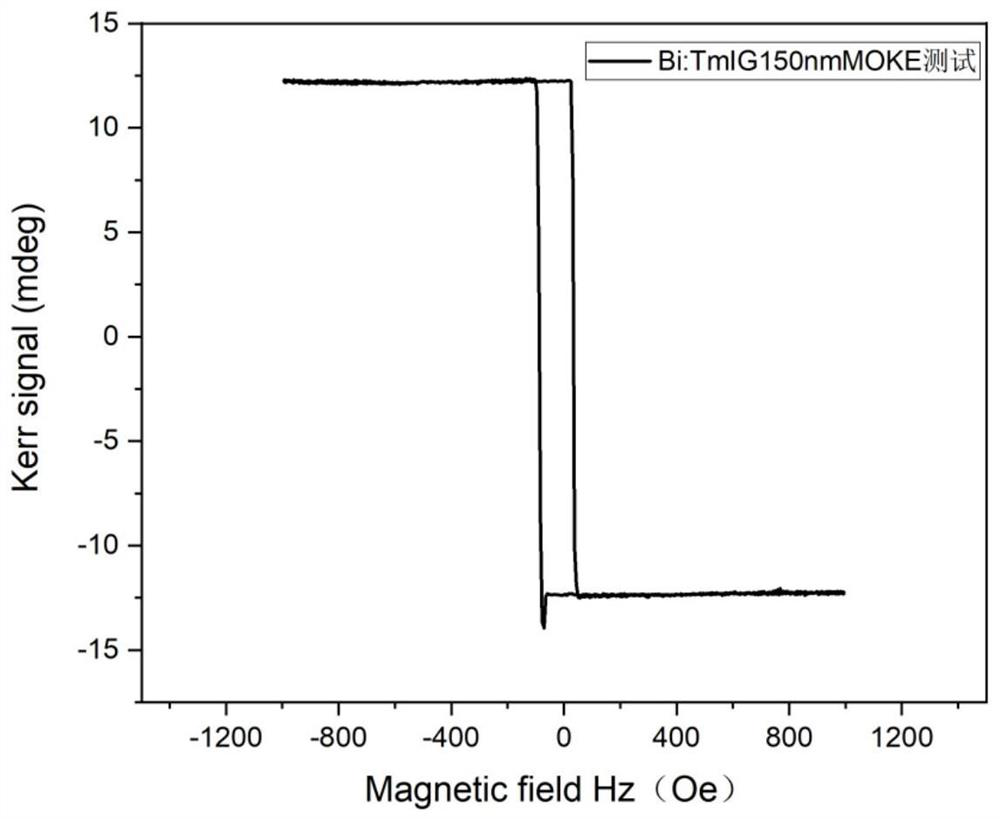
[0039] A method for preparing an alloy / magnetic insulator spin heterojunction device based on GeBi:Pt / Bi:TmIG, wherein the thickness of the heavy metal layer germanium-bismuth-platinum alloy film is 10nm, and the thickness of the magnetic insulating layer Bi:TmIG film is 150nm , including the following steps:
[0040] Step 1. Clean the gadolinium gallium garnet substrate: select the single crystal gadolinium gallium garnet substrate with crystal orientation as the substrate, fix the substrate on the platinum support with platinum wire, and put it into trichlorethylene at 80°C Soak in the solution for 5 minutes, then wash in 80°C deionized water for 10 minutes; then put the substrate into 80°C potassium dichromate sulfuric acid solution for cleaning, and then put the substrate through two 80°C Rinse with deionized water; then soak the substrate in an alkali solution at 80°C (the solution is made of sodium phosphate, sodium carbonate, and potassium hydroxide in a mass ratio of ...
Embodiment 2
[0053] The heterojunction was prepared according to the steps of Example 1, only step 2 was adjusted so that the thickness of the magnetic insulating layer Bi:TmIG thin film was 750 nm, and other steps remained unchanged.
[0054] Among them, the thickness of the magnetic insulating layer is different, the coercive force is different, and the current required for the reversal is different.
PUM
| Property | Measurement | Unit |
|---|---|---|
| Thickness | aaaaa | aaaaa |
| Thickness | aaaaa | aaaaa |
| Thickness | aaaaa | aaaaa |
Abstract
Description
Claims
Application Information
 - R&D Engineer
- R&D Manager
- IP Professional
- Industry Leading Data Capabilities
- Powerful AI technology
- Patent DNA Extraction
Browse by: Latest US Patents, China's latest patents, Technical Efficacy Thesaurus, Application Domain, Technology Topic, Popular Technical Reports.
© 2024 PatSnap. All rights reserved.Legal|Privacy policy|Modern Slavery Act Transparency Statement|Sitemap|About US| Contact US: help@patsnap.com


